Chiplets are revolutionizing the semiconductor industry, enabling unprecedented levels of integration, performance, and flexibility. By breaking complex designs into smaller,…
What happens when a perfectly functioning chip fails to perform in a 3D IC package? As semiconductor designs stack multiple…
What if the most revolutionary advances in semiconductor design aren’t about making things smaller, but about fundamentally reimagining how we…
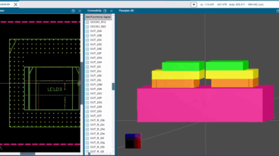
From optimizing connectivity to ensuring electrical performance, designers are tasked with meticulous planning and execution to achieve seamless communication and…
Why is thermal analysis no longer an afterthought in 3D IC design—and what is Siemens doing to empower engineers across…
In this episode of the Siemens 3D IC Podcast Series,we delve into the world of FOWLP (Fan-out wafer-level packaging) with…
In this latest Siemens EDA 3D IC podcast episode, we explore microarchitecture’s crucial role in 3D IC design. Listen in…
The semiconductor industry is rapidly evolving with 3D IC technology and advanced packaging solutions revolutionizing chip design and manufacturing. In…
What is 3D IC technology? 3D IC technology refers to the integration of multiple silicon dies or wafers in a…