Megatrends of advanced IC packaging solutions
Over last 2-3 years, everyone has been talking about Moore’s “Law” becoming invalid. Even if it does, we will continue to reduce the cost of logic gates — just as we did before solid state electronics was developed. This learning curve is forever, it will continue.
Trend #1: Integrate heterogeneous chips
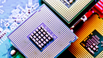
But the reliance we have placed upon shrinking feature sizes to reduce costs will not continue. We will have to innovate in other ways to satisfy the industry demand for the continued increase in electronic functions per unit area. This is what’s driving packaging innovation. One path is to integrate, on package, heterogeneous or homogeneous smaller high-yield chips. DARPA is driving a number of initiatives around chiplets, functional building blocks that when combined provide the same capabilities as a monolithic SoC.
Trend #2: 3D integration across stacks
But having access to even known good chiplets still leaves open questions. Primary among them is, ”What is the best way to combine these chiplets into a working system?” Here we meet a double-edged sword. On the one hand, there are lots of established methods: 2.5D integration on a silicon interposer connected through C4 bumps and TSVs to the ultimate BGAs that connect to the boards. Then there are simpler connections from die to die through super thin, and often very small, bridge-like interposers that do not require TSVs. Then of course there is the well-publicized die-to-die connections through package RDL in the form of wafer-level fan-out processes. Going to full 3D opens up even more options. Two or more components may be stacked with a combination of direct bonding and TSVs. Using through-mold-vias (TMVs), opens more methods to integrate across stacks.
Enabling the future with a High Density Advanced Packaging solution
While some of these approaches, such as CoWoS style using silicon interposers or FoWLP using package RDL, continue to gain in popularity, it is clear that none of these approaches are likely to go away. Ultimately the choice of how to best integrate chiplets will depend on the design requirements. While this seems daunting, it ultimately allows more ways for engineers to differentiate their final offerings.
Of course, one of the big challenges this creates is how to determine which approach ultimately will be best. This is not trivial. The best approach is to digitally prototype the complete package assembly so early predictive analysis can be used to evaluate approach viability.
This drove Siemens EDA to develop its High Density Advanced Packaging (HDAP) solution where a true 3D virtual model of the package assembly can be constructed and then analyzed not only for routability, signal and power integrity, but also for structural performance such as thermal stability and thermally induced stress.
Lessons learned
We learnt that a design solution for this new breed of packaging must be able to cope with a level of design capacity never seen before; yet deliver real-time performance and be available on Windows as well as Linux. To achieve this, we began applying foundry proven technology to an emerging process that is more foundry-like than it is traditional organic laminate package-like.
Of course, foundries capture their IC processes as PDK’s (Process Design Kits) in order for their customers to efficiently design and obtain high-yield results. Therefore, in conjunction with OSAT such as Amkor, the ADK or PADK (Package Assembly Design Kit) was created in order to support and drive the adoption of these new packaging technologies and help fabless semi’s and systems companies to easily transition.
HDAP is the new platform for “More than Moore” to achieve electronic functions per unit area scaling, and Siemens EDA is a committed leading-solution supplier with its Xpedition and Calibre technologies.