If you have not heard of it before, 3Dblox is an emerging standard that was first created by TSMC but is now managed by IEEE.
Innovator3D IC solution suite release 2510 marks a groundbreaking first release of the comprehensive Innovator3D IC solution suite.
With 3D IC integration blurring the lines between chip and package, is your team’s mindset truly system-centric, or are traditional…
The future of semiconductor innovation is rapidly shifting from monolithic chips to advanced, multi-chiplet architectures. As devices demand greater power,…
Would you risk millions of dollars on a semiconductor design without knowing if it can be manufactured? Discover why test…
As 3D IC complexity skyrockets, are we truly evolving our design methodologies at the same pace, or are we unknowingly…
Q: Is dedicated SI/PI analysis still necessary in 3D IC design? A: With the rapid advancements in chip design automation…
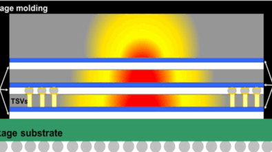
As semiconductor devices grow more powerful and complex, effective thermal management has become a top priority in IC design. With…
Chiplets are revolutionizing the semiconductor industry, enabling unprecedented levels of integration, performance, and flexibility. By breaking complex designs into smaller,…