Siemens partnered with Intel Foundry to develop a STCO centric capability that enables a “smart path” to homogeneous disaggregation using Hierarchical Device Planning and parameterized pin regions.
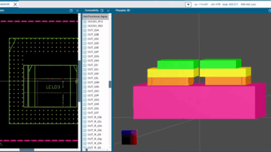
In this blog we will introduce a new way to verify your 2.5/3D IC device assembly level netlist using formal verification that can exhaustively verify all interconnections between the chiplet blocks.
If you have not heard of it before, 3Dblox is an emerging standard that was first created by TSMC but is now managed by IEEE.
Chiplets are revolutionizing the semiconductor industry, enabling unprecedented levels of integration, performance, and flexibility. By breaking complex designs into smaller,…
What is 3D IC technology? 3D IC technology refers to the integration of multiple silicon dies or wafers in a…
Are you struggling to integrate chiplets into an advanced packaging platform due to design fragmentation challenges? The complexity of managing…
In the rapidly evolving semiconductor industry, the drive towards miniaturization and the integration of complex functions through advanced packaging and…
Welcome to a look back at a landmark year in 3D IC technology — 2024 was nothing short of revolutionary!…
Discover how Siemens’ EDA evolution of machine learning in the physical design and verification of semiconductor packages.