Taking 3DIC heterogeneous integration mainstream
October 2, 2024
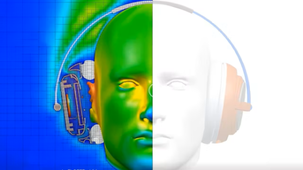
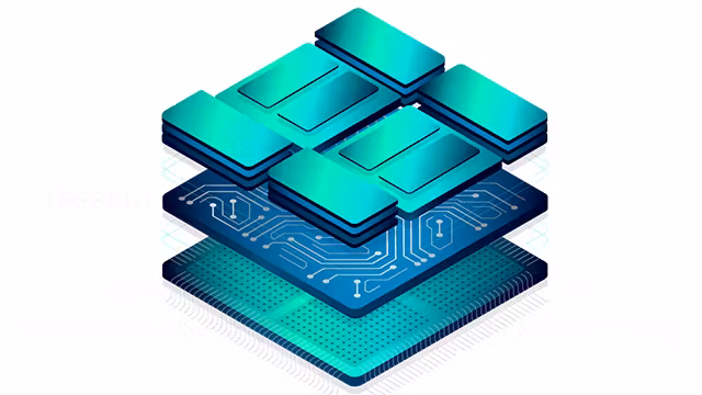
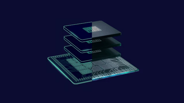
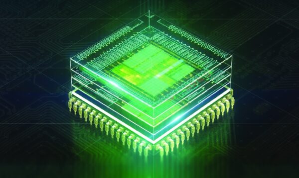
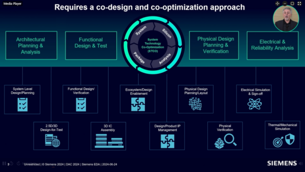
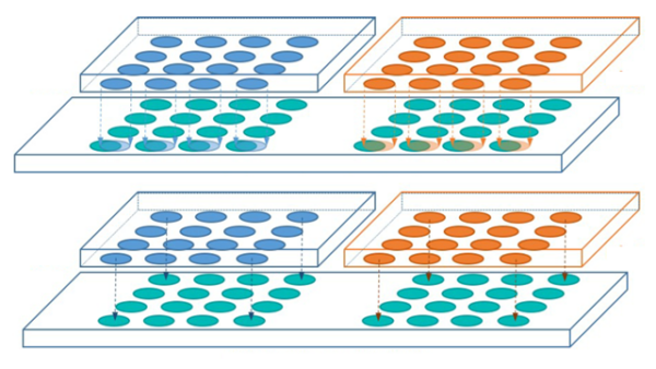
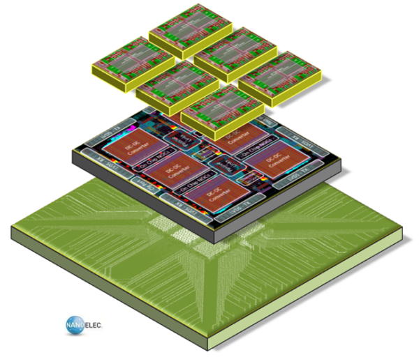
In this presentation, we will explore the challenges introduced by 3DIC, the current state of the industry to address those challenges, the ecosystem needed to support 3DIC, and how users today can successfully adopt 3DIC leveraging new solutions, workflows, and 3DIC Design Kits (3DK) from Siemens EDA that are designed specifically with 3DIC in mind.