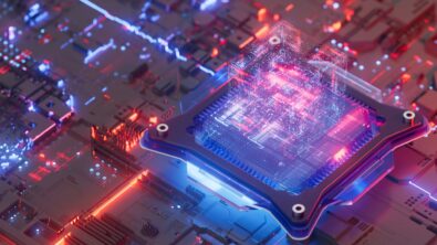
Five Key Trends of Co-Packaged Optics (CPO) in 2026

For years, data-center performance scaled by following a familiar playbook: faster GPUs, higher SerDes rates, and increasingly aggressive board designs. That playbook is no longer holding for today’s AI systems. As AI clusters push beyond 100 Tb/s per node, the gap between what silicon can generate and what traditional copper interconnects can deliver is widening fast.
Three hurdles are now colliding:
- First, power delivery is nearing practical limits. Adding GPUs no longer scales linearly, with power and infrastructure costs rise faster than performance.
- Second, electrical bandwidth is stalling. Even as SerDes speeds increase, copper-based links struggle to deliver the required bandwidth per watt, once equalization and retiming overheads are factored in.
- Third, distance itself has become a problem: latency, energy per bit, and signal integrity degrade sharply with electrical reach.
These pressures are driving renewed momentum behind co-packaged optics (CPO). According to LightCounting, sales of lasers and photonic integrated circuits for optical transceivers are expected to grow from $2.4B in 2023 to $5.9B by 2029, fueled largely by AI data centers.
Read on to learn key CPO trends shaping AI systems in 2026 and the challenges designers will need to solve to make CPO work at scale.
Trend 1. CPO will be essential to lowering AI factories’ power consumptions
AI performance increasingly depends on tightly coupled clusters of XPUs that must operate as a single logical computer. At multi-terabit data rates, interconnect requirements grow combinatorially—systems with millions of endpoints require tens of millions of high-speed links. Electrical interconnects become the limiting factor. Insertion loss rises non-linearly with frequency and distance, forcing increasingly aggressive equalization. Retimers and DSPs can recover signal integrity, but at a steep cost in power consumption. Research predicts that by 2027, AI data centers’ power demand will grow by 50% globally. And about 60% of data center energy is spent on data movement, not compute.
To address the energy demand from AI, co-packaged optics (CPO) brings optical engines directly adjacent to switch ASICs, accelerators, and chiplets. By collapsing electrical distances from inches to millimeters, this proximity reduces power consumption and signal loss while increasing bandwidth density and lowering latency. It leads to a system architecture better suited to modern AI workloads, where thousands of processors must exchange data continuously and behave as a single, tightly coupled machine.
CPOs enable a credible path to sub pJ /bit by placing the optical engine directly adjacent to, or within the same package as the switch ASIC or XPU. NVIDIA’s recent report shows that transitioning from pluggable transceiver to CPO in 1.6T networks can reduce link power from 30 W to 9 W. Industry analyses expect exponential growth in CPO deployments, with 3.2T ports exceeding 10 million units by 2029. Recent platforms underscore how quickly CPO technology is maturing.
From a design perspective, CPO requires teams to adopt high-capacity design and analysis tools capable of handling the complexity of advanced packaging technologies such as 2.5D interposers and hybrid bonding, which enable dense integration of photonic and electronic ICs. Just as importantly, design teams must move toward a true system-technology co-optimization (STCO) flow, where electrical, optical, thermal, and packaging assumptions are evaluated together—early in the architecture phase, before floorplans and integration choices lock in feasibility.
Trend 2. UCIe optical will turn boards and racks into “Extended Packages”
High-speed SerDes-based copper approaches are increasingly strained as insertion loss or crosstalk grow non-linearly with frequency and distance, forcing ever more complex PHY implementations using CTLE, DFE, and retimers. Instead, optical links can maintain bandwidth over centimeter- to meter-scale distances with minimal loss and without heavy equalization.
The UCIe optical will redefine where copper is used. Copper remains a local-reach technology, optimized for in-package communication, while optics take over at package-to-package, board-level, and rack-scale distances. One industry example is Ayar Labs’ UCIe optical interconnect chiplet TeraPHY, delivering 8 Tbps of bandwidth. By pairing optical I/O with UCIe-style interfaces and protocols, such solutions preserve interoperability while extending connectivity beyond copper.
When photonics is integrated directly into the package, the PCB stops being the bottleneck. This enables a more topology-agnostic approach to system design. Modules can be placed where the architecture demands. Boards and racks begin to function as architecturally continuous extensions of the package, optically interconnected and optimized around system intent rather than copper limitations.
Trend 3. CPO’s thermal management drives novel cooling strategies
Although photonic integrated circuits consume less energy per bit than electrical I/O, they are highly temperature-sensitive and introduce new forms of thermal coupling when integrated alongside high-power logic dies. Beyond steady-state conditions, transient thermal behavior becomes critical in CPO architecture as dynamic AI workloads can induce fast, localized temperature excursions that directly impact optical performance.
Cooling strategies optimized for compute alone are often insufficient once photonics are introduced. Designers must manage strong spatial thermal gradients, temperature-induced wavelength drift, laser efficiency degradation, and tightly coupled thermal interactions between electrical and optical components. The high-density packaging imposes more stringent requirements on end-to-end, time-resolved thermal analysis spanning die, package, and system levels, along with careful materials and integration choices.
Trend 4. CPO will demand a transformation in manufacturing and testing
Test scalability is likely to be a primary bottleneck for CPO adoption, as optical and electrical domains impose fundamentally different constraints. Optical signals are highly sensitive to alignment, with micron-scale deviations capable of introducing significant loss, wavelength shift, or measurement error—far tighter tolerances than those typically encountered in electrical test.
This complexity is amplified by the co-integration of waveguides, modulators, photodetectors, and optical sources alongside high-speed digital logic, all of which require precise positioning and mechanically stable interfaces throughout test. In addition, CPO packages may combine optical chiplets from multiple suppliers, each with different materials, optical characteristics, and alignment sensitivities, further increasing test variability. Test teams must shift away from manual, lab-oriented test flows toward automated, production-scale test methodologies capable of delivering accurate, repeatable measurements across both optical and electrical domains.
At the same time, the silicon photonics supply chain must scale. Relative to mature CMOS processes, silicon photonics manufacturing still exhibits higher variability and places greater emphasis on yield and Known-Good-Die assurance. CPO also requires new heterogeneous assembly flows that must be qualified by OSATs and contract manufacturers. Yield excursions at any stage can have an outsized cost impact due to the limited reworkability of co-packaged assemblies.
Trend 5. Standards and ecosystems are still catching up
The CPO supply chain and standards are still evolving, and interoperability across vendors remains a key challenge. Unlike pluggable optics, CPO does not yet benefit from a fully established, interoperable ecosystem; mechanical interfaces, thermal specifications, optical attach methods, and test standards are still evolving. Industry consortia such as Optical Internetworking Forum (OIF) are actively working on establishing common modulation formats and performance benchmarks. Broad ecosystem interoperability will be critical to scaling CPO beyond early, custom deployments.
In parallel, the CPO ecosystem is evolving to address practical manufacturing and deployment challenges. New approaches to fiber coupling and optical alignment—ranging from edge and vertical coupling to advanced passive and active alignment techniques—are being developed to support reliable, high-volume production.
Meeting market expectations and building confidence in co-packaged optics will require more than performance demonstrations. CPO adoption depends on proving robust, multi-vendor business models, along with clear advantages in cost, power, and scalability at the system level. While the underlying technologies are advancing rapidly, key ecosystem elements—including standardized optical interfaces, reusable IP blocks, and interoperable test and qualification flows—are still coming together.
Conclusion
CPO is already reshaping how data-center and AI networks are designed, enabling bandwidth densities and energy efficiencies that copper-based interconnects can no longer deliver. Looking ahead to 2026–2027, the transition from early deployments to broader adoption will hinge on ecosystem maturity as much as technical capability. As standards solidify and manufacturing, thermal, and test challenges are addressed, CPO is positioned to become core infrastructure for AI-scale systems—supporting faster, more efficient, and more sustainable computing.