The hidden heat challenge of 3D ICs: And what designers need to know

Why is thermal analysis no longer an afterthought in 3D IC design—and what is Siemens doing to empower engineers across every step of the process?
In this episode of the Siemens EDA Podcast Series on 3D IC chiplet ecosystems, I welcome András Vass-Varnai, 3D IC Solutions Engineer at Siemens Digital Industries, to spotlight one of the most critical (and often underestimated) challenges in modern chip design: thermal analysis.
What is the role of thermal analysis for 3D ICs?
Andras explains how the shift to 3D IC packaging has dramatically increased power densities and thermal challenges, requiring a fundamental change in how designers approach thermal considerations. The conversation reveals how Siemens is working to bridge the gap between traditionally siloed disciplines by creating integrated tools that enable chip designers, package architects, and thermal analysts to collaborate more effectively throughout the design process.
Whether you’re a silicon designer, package architect, or thermal analyst, this episode offers valuable insights into the future of collaborative thermal modeling, IP protection, and real-time simulation integration. This episode explores how:
- Power densities in 3D ICs approach surface-of-sun magnitudes
- Thermal management can no longer be an afterthought in design
- Different components have vastly different temperature tolerances
- Late-stage thermal issues can cost millions in design changes
- Digital twins enable testing without revealing IP details
Podcast highlights: Key insights from Andras Vass-Varnai
Episode Highlights with Timestamps:
- [02:44] How 3D IC packaging has dramatically complicated thermal analysis challenges
- [04:41] The communication gap between electrical designers and thermal engineers
- [07:39] How poor thermal management can completely disable component operation
- [11:31] BCI-ROM technology for sharing thermal models without revealing IP
- [15:02] The “shift left” approach bringing thermal analysis earlier into design
Watch the full 3D IC technology discussion
Bookmark our 3D IC podcast YouTube playlist for more insights on semiconductor innovation!
Complete episode transcript: The hidden heat challenge of 3D ICs: And what designers need to know
Click here to view the episode transcript
John McMillan (00:01.922)
How important is thermal analysis in 3D IC packaging? Let’s find out. Hello and welcome to the Siemens EDA podcast series on 3D IC chiplet ecosystems brought to you by the Siemens Thought Leadership Team. I’m your host, John McMillan. This podcast series dives into the exciting world of semiconductor chiplet integration and advanced technology platforms using 2.5 and 3D techniques. I talk to industry leaders and subject matter experts to discuss the latest 3D IC industry trends, roadmaps, and uncover how the semiconductor industry is working diligently to make 3DIC mainstream. So whether you’re an engineer, researcher, or tech savvy listener, I’m confident you’ll find this podcast both educational and insightful. If it’s your first time listening to the 3DIC podcast, welcome and welcome back if you’ve been following this podcast series. In today’s podcast, I’m excited to be joined by my special guest, Andras Vass-Varnai. Andres is a 3DIC solutions engineer at Siemens Digital Industries.
And today we’re going to dive into a very hot topic in the world of 3D IC packaging, thermal analysis. Welcome Andras to the 3D IC podcast. And before we dive into today’s discussion, please give the listeners tell a little bit about yourself, your background and your current role here at Siemens EDA.
Andras Vass-Varnai (01:20.066):
Thank you, John. Thank you for having me and it’s very nice to meet you. My name is András Vass-Varnai, and I work on a newly formed team called Central Engineering Solutions, which is aimed at connecting different tools within our EDA organization, connecting design, both chip level design and package level design and architectural tools with multi-physics simulation tools. My role currently is to figure out how to add thermal management and also stress simulations later on to the multi-physics design and verification flow of 2.5D 3D IC packages.
My background is mostly thermal management. I’ve been working in this field for about 17 years. And I came from a university department which put a lot of emphasis on researching semiconductor thermal problems, not just digital components, but also LEDs, power modules, and essentially anything semiconductor. Because if they get hot, their reliability will be heavily impacted.
John McMillan (02:29.336):
Great, thanks. Again, I’m really excited you could join the podcast today and discuss how things are really heating up in the 3D IC designs. Let’s just jump right in. So how is the shift to 3D IC packaging affecting thermal analysis?
Andras Vass-Varnai (02:44.876):
That’s a great question, John. So things have just gotten more complicated, which I don’t think is a surprise to anyone who’s been involved with these advanced packaging technologies. Traditionally, packaging thermal often used to be an afterthought, which wasn’t really done by the design engineers themselves, but there were silos. So you had the silicon engineers, you had packaging engineers, they all did their jobs. And then thermal was maybe considered as a, you know, back of the envelope calculation upfront sometimes, but often people would just go by rules. And at the end of the day, thermal verification and thermal management was really handled by the thermal analyst and thermal measurement persona. So.
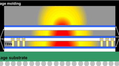
Currently with 2.5D, 3D architectures as you have multiple chiplets packaged together in very close proximity, often stacked on the top of one another, power densities are going through the roof. Actually, we are literally getting somewhere in the order of the magnitude of the power density on the surface of the sun. So that’s crazy to imagine. And that heat has to be let out of the package. We have to make sure that different components don’t impact each other or one another. The cross-heating is minimized. So thermal management can’t be an afterthought anymore. It has to be constant. Early on in the design stage. And this is what our team is trying to help design engineers with, bringing thermal management, thermal engineering closer to them, even those who’ve never done it before.
John McMillan (04:32.878):
So what is the problem with how thermal analysis is being carried out now?
Andras Vass-Varnai (04:41.324):
Well, first of all, it’s difficult. The problem currently or traditionally is there are some thermal engineers, thermal analysts who are really good at what they are doing, but they are not really part of the design process and they don’t necessarily even understand what the designers do. So a silicon design engineer or a package architect, these are traditionally electrical disciplines which doesn’t really correlate to thermal because very traditionally thermal engineering is a mechanical discipline. One key element and key problem within the industry is people don’t really speak each other’s language. So there is a need for tools which help bridge that gap, which enable data seamlessly to be transferred from silicon package or a thermal person and you know you can just log into the same tool either check out the data yourself or have a very detailed request or very very definitive request to your corresponding persona maybe sitting in a different design team so I think one of the big problems is that you have to consider thermal management as part of the design. The designers don’t really always know how to do it. And it’s not easy for them to sync up with the thermal persona either. This is something I’ve been seeing in the industry for a while.
And even building models, you know, the more complex these packages become, the harder it gets, the longer it takes to build a thermal model. Essentially, you need to define every single die or chiplet, every single interconnect, every substrate and interposer in details. And even those details really depend on what you are trying to do.
Andras Vass-Varnai (06:44.156):
They can be very fine details when you’re looking for like a final sign-off type of analysis, or there can be less details when you’re doing an architecture. So you need to be able to figure out what details you need. You need to be able to get the data, have access to the data, and then you need to build that model. And at the moment, very often it’s done manually at the end of the process. So that’s another issue I’m seeing. And ideally, if you were to change that, synchronizing the design process with building the thermal model as a design gets updated the thermal model should be updated as automatically as possible that would enable all of the personas I mentioned earlier to get easier access to simulation in my opinion.
John McMillan (07:31.15):
Okay, cool. So what is the significance of having these thermal models for the customers?
Andras Vass-Varnai (07:39.704):
The significance is at least two-fold. So first of all, when you’re designing something and you’re looking at thermal management, it will impact operation. So bad thermal management can fully disable the correct operation of a component.
And if I start with the design engineers from their perspective, if they find out at the sign-off stage that thermal management wasn’t considered correctly, for example, if you have a high power density, high temperature compute die, like a GPU or a CPU in very close proximately to a high bandwidth memory, excuse me, these devices have different temperature tolerances. So typically high power digital logic could operate up to 110, even sometimes they say 130, 150 degrees Celsius at the maximum, call it junction temperature.
An HBM memory typically operates in the range of 80, maximum 90 degrees. Otherwise, you’ll start seeing problems with the saved data. So if you have these two components very close to each other, it’s good on one hand because the data transfer rate may be a bit higher, the speeds will be a bit higher, signal integrity will get better. But on the other hand, there is a trade-off, there is a potential cross-heating from one die to the other die and if you get your memory too hot and it’s really hard or maybe you don’t find any way at the end of the design process to keep it cool enough your design will not be feasible and if you you already are far enough very close to the sign-off, you may need to track back and the design changes can cost a lot of money. I mean, we are talking about potentially millions of dollars at that stage. So engineers are under a lot of stress, unfortunately, to make sure that they do this right. And I think it’s very important for us to help them.
So that’s the design persona. Now, there’s another side, of course, which are the customers, so the end users of the components and from their perspective they want to make sure that the designers have done their job well because if the job wasn’t done well then reliability, lifetime, long activity of the component will be impacted too even if it starts off or starts up correctly on the long run, it may break earlier than it should. So they want to get two things. They want to get validation data, making sure that the design was created correctly. But also what they want to do is get a digital twin, get a thermal model and test it or verify it in their own environment. So for thermal it’s very important how the environment looks like. Maybe a big heat sink or a better thermal interface material can help. So the end user needs to understand how they should do their design.
And the problem is if we were to give them a digital twin that might provide a lot of access to IP. So if you look at the thermal model, you get die sizes, get heating the area locations, you get a lot of details of how the package looks like, and no semiconductor company wants that. So we’ve been working on a way, our Flotherm team has pioneered the technology called BCI-ROM, boundary condition independently used order model, which maintains the thermal descriptive nature of the model, but it hides all the physical details, all the IP and our customers can either use it in Flotherm, we call it embeddable BCI-ROM or in mathematical tools to create different types of predictive models without the manufacturer of the component needing to be worried about IP leaking out. So that’s kind of the dynamics within the supply chain at the moment.
John McMillan (12:11.778):
Well, gotcha. So what would you say is Siemens vision for the idea of future workflow?
Andras Vass-Varnai (12:20.694):
Well, the vision is first of all connecting both vendors and their customers and all of these are our customers in a larger ecosystem, supporting that supply chain, which I just described right before.
That’s certainly something we’re trying to do and we’re looking at market areas which we believe are very important for specifically 2.5D 3D ICs. One is automotive, so we see more and more demand for these cheap led-based architectures in autonomous vehicles, ADAS systems, so making cars more intelligent and being able to make decisions directly on board instead of doing it in the cloud. That’s one application where you have the chips, but they have to be cooled all the way to the system level. And the other one is data centers. I mean, everybody probably listening to this podcast has been exposed to AI and all these assistants. We’re really creeping into our lives today, but those require very high compute power and it’s a core design of very complex packages, printed circuit boards, subsystems, systems, and all of these would go into a data center and you go from chip level cooling to system level liquid cooling. So bridging all those gaps is one of our visions.
Within the design community, so working for Siemens EDA are immediate direct customers, are the designers, the design community. For them, the vision is to have their daily job by connecting those three personas I mentioned earlier, enable the chip designer, the package architect and the thermal analysts to work together very closely, be able to exchange data seamlessly. And ultimately at the end of the day, make sure that the design itself as it’s being evolved from an architectural phase through in-design all the way to final sign-off. Every time a change happens, we should be aware of it and we should be able to update the thermal model, which essentially acts as a digital twin of the design in its current stage. So that’s the ultimate goal which we would like to achieve.
John McMillan (14:49.39):
Gotcha. Are you describing like kind of integrated shift left technologies, kind like we’re seeing in other areas of design, electronics design?
Andras Vass-Varnai (15:02.796):
That’s right. That’s a very good way to put it. It’s kind of a shift left or a democratization. So we have engineers in the design process who never ever really encountered thermal management, such as die designers. They would do their floor planning, but in the past it wasn’t really thermally driven.
John McMillan (15:06.648):
Okay.
Andras Vass-Varnai (15:25.28):
It was a factor and people would look at it. Maybe not most of the die designers, but today with chiplets and specifically chiplets being stacked on the top of each other, it matters more and more where high power IP blocks are placed. We have a solution called Calibre3D Thermal, which was specifically designed for this kind of user persona. It’s based on existing Calibre technologies which they are very well aware of for their verification flows. But at the same time it’s combined with technologies coming from Flotherm, Simcenter Flotherm, which is our flagship thermal tool. So Calibre 3D thermal can read these die databases, can translate them into a high fidelity thermal model and can support those personas who haven’t really done thermal simulation yet to do thermal simulations with ease and get a map, a temperature map or a temperature histogram.
Now, that’s the die designer team. When it comes to the package architects, they will use these dies, they will put them on an interposer, they might put that interposer on a package substrate, and all of these will impact thermal management. So, from their perspective, they would like to understand how they should be placing the different chiplets. And typically they look at connectivity, they look at different electrical factors, but again, thermal very often is either not considered in the past or it’s just an afterthought. So what we are trying to do with the same toolkit, we have a design cockpit called Innovator 3D IC, which can integrate together with Calibre3D thermal, and the database which is built up, the connectivity which is designed in Innovator 3D IC can be translated also into a thermal model. So using the same backbone for the full connectivity stack we can do another thermal analysis and this way the package architect will get an understanding of their design.
Andras Vass-Varnai (17:39.384):
But of course we talk about the end users, we talked about system level thermal models, so all of those have to be done as well. And that’s our Flotherm user persona. They are the hardcore thermal guys, the mechanical engineers who do this for a living. And the way we’re trying to help them is in the past they would get the specification, they would go into their tool, they would build up a model really from scratch. There is no need to do that anymore because the former two persona, their designs will be seamlessly transferred into a Flotherm compliant model.
And once the design is either ready or it’s being reiterated with an innovator 3D IC, we can connect that to Flotherm and every time a change happens, check out the new Flotherm model so the system level person doesn’t need to build up that model anymore. But he or she will be able to use what their colleagues were doing upstream. And this way, all these three personas will be fully connected through a digital twin.
John McMillan (18:51.214):
Gotcha, great, great information. Thanks, Andres. This has been very insightful, very informative for me, and I hope it has been for the listeners as well. I want to thank you for joining me today and sharing your knowledge and thoughts on this very important aspect of 3D IC packaging. Any last comments before we close the podcast?
Andras Vass-Varnai (19:10.232):
I just would like to say, John, it’s been pleasure talking to you and I really hope that thermal, thank you, I really hope that thermal management will move away from being an afterthought to something which people very, very commonly do and I really hope our tools will make it easier for them.
John McMillan (19:28.93):
Hey to all our listeners and viewers, I hope you found this podcast as educational and informative as I know I have. That’s it for today’s episode of the 3DIC Podcast. Thank you for joining us today. Also, be sure to check out the show notes to learn more about today’s topic. And don’t forget to subscribe so you don’t miss the next episode of 3DIC Podcast brought to you by Siemens EDA. Thanks again.
Andras Vass-Varnai (19:51.234):
Thank you.
Explore Siemens 3D IC Expertise, Resources and Solutions
Take the next step in your 3D IC journey by tapping into expert insights, technical content, and advanced design tools from Siemens EDA.
Connect with industry experts
Andras Vass-Varnai Ph.D., 3DIC Solutions Engineer at Siemens EDA – LinkedIn
John McMillan, Siemens EDA – LinkedIn
Access 3D IC Innovation Resources
Stay informed with the latest thinking in advanced packaging:
- Bookmark the 3D IC podcast playlist
- Visit the 3D IC design and packaging solutions page
- Access our 3D IC technical resource library
- Explore Innovator3D IC, the unified cockpit for design planning
Siemens 3D IC design solution
Transform your semiconductor design flow with our full-stack capabilities:
- Heterogeneous 2.5/3D integration
- 3D SoIC implementation
- Substrate implementation
- Functional verification
- Electrical simulation & sign-off
- Mechanical co-design
- Physical verification
- Thermal/mechanical simulation
- Product lifecycle management
- 2.5D/3D design-for-test
- Verification IP for 3D IC
- 3D IC design & verification
- Design for reliability