Navigating ESD challenges in 2.5D/3D ICs: A guide to robust automated verification
By Dina Medhat
Electrostatic discharge (ESD) events cause severe damage to unprotected integrated circuits (ICs). ESD events cause severe damage to ICs due to a sudden and unexpected flow of electrical current between two electrically charged objects. This current may be caused by contact, an electrical short, or dielectric breakdown.
No matter the cause, all ESD events can cause a metal melt, junction breakdown, or oxide failure. ESD can damage an electronic component at any stage of its production or real-world use if not properly prevented. ESD events can cause ICs to fail prematurely, or to operate at less than designed functionality, neither of which is good for market reputation.
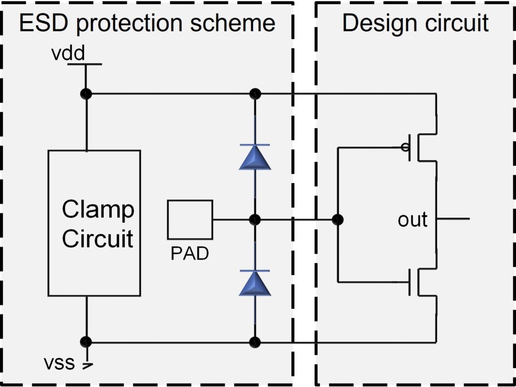
You already know that, of course, because you’re required to add ESD protection schemes (like in figure 1) on both the schematic and layout, following ESD design rules included in design rule manuals. But now you’re faced with providing ESD protection for a 2.5D or 3D IC design. What do you do? You can use the new Calibre 3DPERC (die2die) methodology for automated ESD verification that effectively and accurately addresses the emerging challenges for ESD robustness in 2.5/3D IC designs.
About 2.5D and 3D ICs
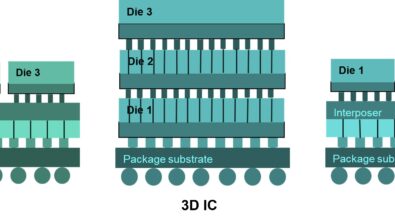
2.5D/3D ICs have evolved into an innovative solution for many design and integration challenges. 2.5D ICs have multiple dies placed side-by-side on a passive silicon interposer. The interposer is placed on a ball grid array (BGA) organic substrate, micro-bumps attach each die to the interposer, and flip-chip (C4) bumps attach the interposer to the BGA substrate. In 3D ICs, dies are mounted on top of each other, there are interfaces for communication between dies, and through-silicon vias (TSVs) are used for communication with the substrate. Figure 2 illustrates the difference.

Challenges of ESD verification for 2.5D/3D ICs
So, can you just assume that 2.5D/3D ICs have the same ESD verification challenges as 2DICs? The short answer is no. Automating ESD Verification in 2.5D/3D ICs introduces additional challenges which are not in 2D “traditional single die” ICs. Industry white papers and IEEE publications have outlined and provided extensive background material for many of these challenges. Like differentiation between IO types, corresponding HBM/CDM constraints, working with a mix of different technology nodes and foundries, and taking care of different ESD methodologies.
ESD robustness requires evaluating ESD protection for correct construction and interconnect robustness. Two areas are evaluated for interconnect robustness: point-to-point (P2P) parasitic resistance and current density (CD).
Measuring P2P resistance requires calculating the interconnect resistance between a given external pad (or cell port) and the corresponding ESD device pin and report the total resistance. Measuring CD requires calculating the current density in every polygon on every metal/via layer from a starting pin (or port) to an end pin (or port) by injecting an appropriate current at an external pad and measuring CD on all interconnect polygons up to the ESD device pin.
Designers need a systematic methodology to address ESD challenges and verify the ESD robustness of 2.5D and 3D ICs using an automated process that includes interconnect ESD P2P/CD verification. Fortunately, Siemens’ Calibre has just the thing.
Our solution: Calibre 3DPERC (die2die) for automated ESD verification for 2.5/3D IC designs
At Siemens EDA, we formulated a systematic methodology to verify the ESD robustness of 2.5D and 3D ICs that can be implemented using Calibre 3DPERC (die2die). It starts by performing die/interposer ESD verification using Calibre PERC, followed by assembly analysis using Calibre 3DSTACK. The output is system-level interconnect P2P/CD results.
Inputs for this verification methodology are:
- Layouts of every die/interposer.
- ESD P2P/CD results database for every die/interposer.
- Assembly rules file (die/interposer definitions and stack configuration).
- ESD P2P/CD experiments rules for the 3DIC design.
Outputs are:
- Assembly layout
- ESD violations database
- ESD violations report
The bottom line on ESD robustness in 2.5D and 3D ICs
ESD protection is an essential element in IC designs. While automated verification of the accuracy and capacity of an ESD protection circuit is an established process for 2D IC layouts, 2.5D/3D IC design ESD protection verification must overcome additional challenges that, until now, have resisted automation.
New automated ESD verification methodology effectively and accurately addresses the emerging challenges for ESD robustness in 2.5/3D IC designs and is available in Calibre 3DPERC (die2die). Moreover, we’ve introduced 3D-aware die analysis to efficiently support hybrid bond technology. Ensuring accurate and consistent ESD protection in 2.5/3D ICs raises the reliability and product life of these products, ensuring they deliver the value and functionality the market demands.
Interested in the details? Download a copy of our technical paper, ESD Verification for 2.5D and 3D ICs.
