Navigating 3D IC stress: physical realities and best practices for 3D IC reliability

By Shetha Nolke
As the semiconductor industry shifts toward heterogeneous 3D ICs, exciting benefits are coming within reach—from smaller footprints to higher performance and lower power. But with every leap in integration, new reliability challenges emerge—especially when it comes to stress at the device and package level. Here’s a closer look at why stress matters so much in 3D ICs, what can go wrong and how engineering teams can stay ahead of the curve.
The rise of heterogeneous 3D ICs
Heterogeneous 3D IC design lets engineers break up a system into specialized blocks—placing high-performance circuitry on advanced nodes, while less critical functions use established, cost-effective technologies. This “dis-integration” unlocks powerful new options for tradeoffs. Smaller packages, reduced power budgets and tailored feature partitions are all in play. It’s a shift impacting everything from cloud CPUs to IoT sensors.
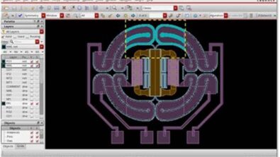
The catch? As designers connect dies and chiplets in all three dimensions, each decision comes with its own set of risks. It’s not just about mapping functionality—it’s about making tough calls between performance, reliability and manufacturability. Some mechanical failures are obvious, like die cracking, solder fatigue, warpage or delamination (see Figure 1), but others—like subtle stress effects that impact device physics—can be much harder to spot.

Managing the new challenges of 3D ICs is a major project of the entire semiconductor industry. As an example, Siemens recently expanded our collaboration with TSMC to address the challenges and opportunities presented by this emerging technology.
Stress risks: visible and hidden threats
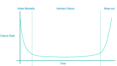
Some of the risks posed by 3D packaging are well known, prompting changes in assembly methods and material choices. But as new device and package combinations come online, new failure modes keep appearing. Mechanical loads imposed during assembly—especially during chip reflow processes, where temperatures spike well above normal SoC limits—interact with thin dies and diverse metals and dielectrics to heighten the risk of fault. Mechanical issues don’t just mean cracks and delamination; due to the piezoresistive effect, they can also cause electrical behavior to shift unexpectedly.
And not all devices respond to stress the same way. Circuits based on piezoelectric properties or those intended for critical use (think automotive, health or infrastructure sensors) are especially vulnerable. For these applications, both the packaging process and broad operating temperature swings need to be factored into reliability checks right from the start. Waiting until sign-off risks serious issues—early, physics-driven validation has never been more important.
Evaluating stress: why collaboration and detail matter
On paper, figuring out stress in a 3D assembly might sound straightforward—it seems like a matter of plugging in physical models. In practice, defining the package for simulation is a complex, team-based challenge.
Start with the basics: packages span everything from millimeter-scale substrates down to nanometer-scale chip features. Both chip and packaging engineers need to describe and share details of every physical component, a process made easier by standards like 3Dblox but still demanding accuracy and modular thinking. At early design stages, some details may be missing, so “best guess” assumptions about materials, layer thickness, or routing are often needed. These assumptions feed initial stress simulations, which are refined as new information becomes available—sometimes over months or even years.

Who actually models these stresses? Sometimes it’s the IC design team, sometimes the packaging experts, each bringing a different view of what’s important. The best outcomes arise from collaborative co-optimization, balancing perspectives and risks across the design.
The material and process challenge
Defining accurate material properties is another sticking point. It’s tempting to treat unknowns as simple “black boxes”—for example, assuming an IC is just a chunk of silicon. While this provides a starting point, it can miss out on key physical nuances, especially as intellectual property or proprietary material stacks come into play. More detailed descriptions mean more accurate stress results.
Beyond just geometry and composition, the assembly process itself can impart stress at multiple points. As temperatures spike during reflow or annealing, different materials contract and expand at different rates, transferring stress into adjacent layers. Knowing typical and peak process temperatures and where localized heating (like under BGA solder balls) might occur, means fewer surprises in simulation.
Once the package and its properties are defined as fully as possible, finite element analysis (FEA) can be used to calculate resulting stress fields—starting a feedback loop of simulation, evaluation and design improvement.
Making sense of stress analysis results
Once stress across the package is modeled, how should results be interpreted? Early on, sweeping go/no-go checks can quickly flag material limits or risky stack-ups, prompting immediate refinement or iteration. Spending time on package composition while design freedom remains is a powerful way to rule out high-risk scenarios with minimal sunk cost.
As the product matures, analysis shifts to specifics—evaluating chip-package interfaces, performing “what-if” simulations for critical device locations and finally, running sign-off confirmation that reliability targets are met. Visual tools let engineers explore stress distributions globally or in detail, flagging things like warpage, offset and even mobility impacts.

Going one step further, piezoresistive effects can be modeled and back-annotated to the schematic or netlist, allowing stress-aware checking of circuit performance via downstream verification like LVS.
Looking ahead: navigating complexity together
The transition to heterogeneous design and 3D packaging has introduced a level of physical complexity not seen in previous technology generations. The interplay of mechanical and electrical effects—and the need to account for them early and often—will only increase as more sophisticated stacks come online. As always, physics sets the boundaries engineers work within and margin for error continues to shrink.
Driving reliable, manufacturable 3D IC products forward will require the combined ingenuity of chip designers, packaging teams and process experts—united by collaborative modeling, robust standards and a willingness to continually revisit assumptions as new risks are discovered. In this era, physical stress isn’t just a variable; it’s a vital ingredient for every meaningful design—and the teams that master it will set the pace for innovation to come.
For a more in-depth look at this topic, download our paper Thermo-mechanical stress on active chiplets in a 3D IC heterogeneous package assembly.