Cracking the code: ensuring reliability and performance in IC design with EM/IR analysis
By Karen Chow and Joel Mercier
Integrated circuits (ICs) are everywhere, powering everything from washing machines and TVs to medical devices and military technology. And in this vast world of integrated circuits, reliability is key – it’s what keeps our creations ticking in all these different applications. Think about it: when people buy stuff, they want it to last, right? But in critical systems, like medical devices or military tech, reliability isn’t just a bonus – it’s mandatory.
Now let’s get more specific… electrical reliability is a different story compared to mechanical reliability. While the movement of mechanics can wear down over time, integrated circuits don’t have moving parts. Instead, we deal with things like electrostatic discharge, electromigration, and the wild swings in voltage and temperature. Making an IC that lasts isn’t easy, especially when you’re cramming billions of transistors onto a tiny chip. The smaller we go with our tech, the more we pack in there, which means more challenges for us to tackle – but that’s what keeps it interesting.
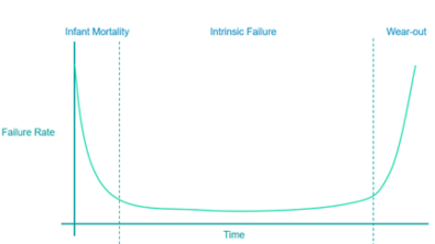
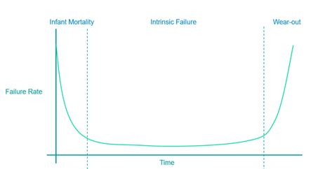
IC reliability can be understood using the “bathtub curve,” splitting into three key phases: the baby phase, the regular, or “normal” phase, and then the “farewell tour” (check out Figure 1 for the visual). This curve isn’t just for ICs; it’s a big deal in all things reliability, showing us when stuff is likely to call it quits. Phase one is like the infancy of our chip, where the failure rate drops quickly as process quirks and factory hiccups are ironed out. Phase two is when the IC is doing its thing with a low, random failure rate – this is the longest stretch of its life. Then, phase three creeps in with the wear and tear, thanks to oxide and interconnect issues caused by a little something called electromigration (EM).
Electromigration: The ugly truth
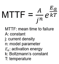
EM refers to the movement of metal atoms triggered by the passage of electric current through a metal. This phenomenon occurs as electrons in the metal carry momentum, transferring it to metal atoms upon collision within interconnects. Over time, this movement can create voids or hillocks in the metal paths, potentially leading to open circuits or short circuits, respectively. The risk of EM is directly linked to the current density in these paths; higher current densities increase the likelihood of EM-related failures. Engineers often use simulations to predict EM-induced failures by analyzing current flow and identifying areas with excessive current densities, such as vias. Other influencing factors include wire material, temperature, and size. Black’s equation aids in quantifying these factors to estimate the mean time to failure (MTTF) of an IC due to EM.
The escalating concern surrounding electromigration stems from its heightened impact in modern IC designs with advanced process nodes. As transistors shrink, interconnects must also reduce in size, leading to higher resistance and current densities that make them more susceptible to EM. Furthermore, the trend of transistor scaling exacerbates self-heating issues, particularly evident in silicon-on-insulator (SOI) fin field-effect transistor (finFET) and gate-all-around field-effect transistor (GAAFET) technologies. These devices, due to their three-dimensional structures and limited heat dissipation paths caused by thick buried oxide layers, trap internal heat within the interconnects, accelerating the EM effect. For instance, a 7 nm finFET can experience a temperature rise of 12K, while a 5 nm GAAFET can rise by 17K, significantly reducing the time to failure of interconnects due to EM by up to 38% in SOI finFETs and 45% in GAAFET technologies.
Survival guide for IC designers to limit electromigration
- Wire width:
- Making interconnects wider can help handle current better, but this clashes with scaling designs down, especially in today’s advanced nodes.
- Wire material:
- The semiconductor world shifted from aluminum to copper about 25 years ago because copper handles current way better and fights off electromigration (EM) like a champ. But even copper has its limits as designs keep getting smaller.
- Barrier/Seed layers:
- EM occurs at the edges of wires where the copper and dielectric meet, so designers throw in a barrier or seed layer between the copper and dielectric. This layer, often a mix of copper and other metals like cadmium or zinc, boosts their bond and reduces boundary EM drama.
- Blech effect:
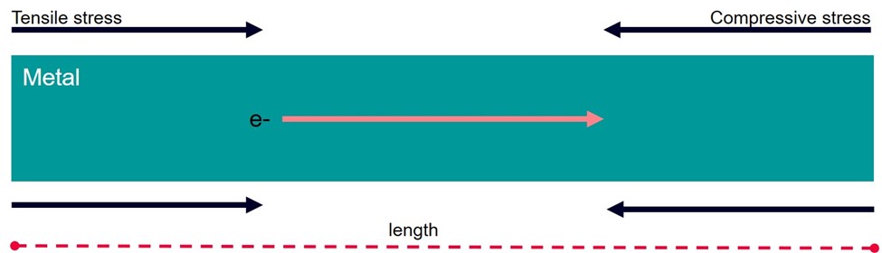
- Back in the ’70s, Ilan Blech figured out a neat trick to fight EM, now known as the Blech effect. It’s like this: when electrons migrate, they put a strain on wires – tensile stress at one end, compressive at the other. This stress actually helps because it makes the wire walls stronger, slowing down migration. Blech even found a sweet spot called the Blech length, around 10 to 100 microns long, where no migration happens. So, by keeping interconnects within this length, designers can keep EM at bay.
IR drop – What is it and why is it important?
IR drop is essentially a voltage reduction caused by the resistance encountered by current as it travels through wires. This phenomenon is governed by Ohm’s law, where voltage (V) equals current (I) multiplied by resistance (R). As chips evolve with device scaling, their components, like transistors and wires, shrink in size but the overall chip dimensions remain relatively constant. This scaling discrepancy results in narrower wires that maintain their length, leading to increased parasitic resistance in these wires. Consequently, the voltage along the path from a supply pin to the input of a cell decreases due to this heightened resistance. This resistance keeps escalating as the industry pushes designs into ever-smaller nodes. For instance, transitioning from a 28n m chip design to a 7 nm one can yield a tenfold increase in wire resistance.
There are two main types of IR drop in chip designs: static and dynamic. Static IR drop occurs due to constant current draw, stemming from parasitic resistance in wires. On the other hand, dynamic IR drop emerges from the intense switching activity of transistors, generating high-current zones that cause voltage drops. As chip power consumption and frequency increase, particularly in advanced nodes, dynamic IR drop worsens. This is because more transistors switch simultaneously, creating localized areas of high current and time-based voltage dips.
Watch more about dynamic EM/IR analysis with our short video Dynamic EM/IR analysis on large analog circuits with mPower (siemens.com)
Understanding and addressing IR drop is crucial for chip designers. Voltage drops can slow down transistor operation, leading to timing violations and potential performance issues in the final chip. Furthermore, chips that fail to meet design specifications may need to be sold at lower prices for less-demanding applications, impacting revenue. To combat IR drop, designers employ techniques like widening metal wires and adding vias to reduce static IR drop. For dynamic IR drop, strategies include integrating decoupling capacitor (DCAP) cells to manage voltage spikes during switching and adjusting device settings to control localized current spikes. These efforts aim to minimize IR drop and optimize chip performance and reliability.
The role of parasitic extraction in IC reliability
Parasitic extraction is all about tackling the unintentional electrical hiccups that pop up in IC designs. These “parasitics” come in different flavors – resistance, capacitance, and inductance – and can mess with a chip’s performance.
Let’s break it down:
- Parasitic resistance:
It’s like the traffic jam for electrons, making data loss or glitches possible. Designers play around with current levels and wire configurations (like adding vias or using thicker traces) to ease this resistance headache. - Parasitic capacitance:
Imagine unintended electrical “hugs” between circuit conductors causing signal distortions. This is a big deal, especially for speedy circuits. To combat it, engineers tweak spacing and use special materials to reduce these unwanted “hugs.” - Parasitic inductance:
This sneaky one can delay signals and use more power. Shorter, thicker interconnects kept close to the ground can help minimize this pesky inductance.
Now, onto the tools that make sense of these parasitics:
Calibre xACT:
The Calibre xACT tool dives deep into EM-induced resistance drops, predicting and preventing device failures caused by EM. It sniffs out all the parasitics and intentional components, generating a netlist that helps designers fine-tune layouts for optimal performance.
mPower platform:
The mPower platform is the power player for IR-drop, power, and EM analysis. It’s like the detective that finds the EM/IR hotspots in your circuit, helping you tweak layouts and run simulations to fix any issues. It works hand-in-hand with extraction tools like Calibre xACT to ensure your design meets the mark for performance and reliability.
Watch our video on how EM/IR analysis helps designers from block to full-chip Effective EM/IR analysis for FPGA designs using Siemens mPower Analog
Conclusion
EM and IR drop can throw a curve ball at your IC’s performance and reliability plans. However, figuring out what’s causing these issues and tweaking designs is key to making sure your chips perform as expected once they’re made. To do this right and on time, design teams need reliable EDA tools that can quickly detect those parasitics and analyze EM/IR – that’s the secret for nailing down those designs and hitting tapeout with confidence.