How to verify well layer connectivity with soft checks
By Terry Meeks
In the landscape of modern IC chip verification, ensuring the connectivity from diffusion layers to well regions is critical for the proper functioning of integrated circuits (ICs). If power or ground are not connected correctly, the chip will fail. Soft checks, a specific type of Electrical Rules Check (ERC), play a pivotal role in examining this connectivity, preventing conflicts, and ensuring the integrity of power and ground nets. Let’s delve into the nuances of soft checks and the methodologies for efficient detection and debugging.
Unpacking the notion of “soft checks”
A “soft check” refers to an ERC that scrutinizes the connectivity from the diffusion layers to the well (substrate) regions of the IC design. Referred to as “stamping,” soft connectivity connects an upper layer to a lower layer without allowing the connectivity from the lower layer to affect other upper layer polygons. A soft check evaluates this soft connection to identify and report any conflicting shapes. The primary objective of soft checks is to ensure that all of the well regions are connected to power or ground through the metal layers to the diffusion taps, eliminating device connections through the well layers.
Understanding well layer connectivity
The importance of well layer connectivity is often underestimated in IC design. Some digital designs may simplify connectivity verification by having one power and one ground voltage. Many modern designs, especially analog ones, involve multiple voltages, making well connectivity more complex. Additionally, as process nodes shrink, analog effects become more prominent, adding complexity to well layer connectivity modeling.
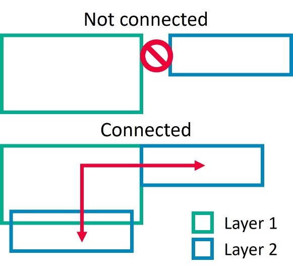
Connectivity between layers in an IC layout is typically determined by assigning the same net identifier when the polygons in those layers touch or overlap. This connectivity must be a two-way relationship that connects the polygons in both directions (figure 1).
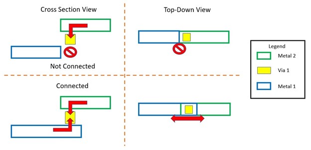
When there is an intermediate connecting layer like a contact or via, the behavior of the connect function is a little bit different. In that case, the three layers must all overlap at the same location, as shown in figure 2.
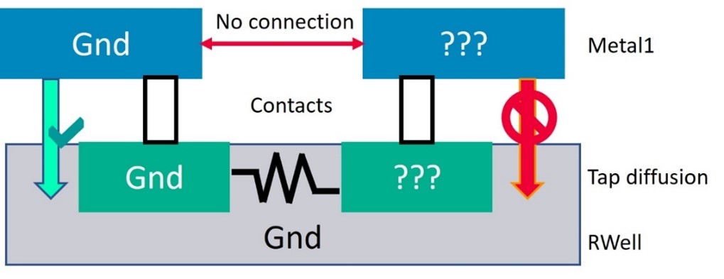
Soft connectivity from diffusion to well layers
Well layers should not be used to conduct signals due to their lower doping concentration. Soft connectivity, often termed “stamping,” creates a one-way connection from an upper layer to a lower well layer, avoiding high-resistance connections.
Soft connectivity from diffusion layers to well layers involves a direct, two-layer event. N+ and P+ implanted diffusion regions within NWell and PWell regions, respectively, conduct current. In figure 3, the connection shown on the left side has Metal1 (named Gnd) connect through a contact to a diffusion region over a like-biased well region (N+ to NWell, or P+ to PWell), which is known as a tap diffusion. The metal layer closest to the tap diffusion shapes connects through a contact opening layer, situated above the diffusion layer. This connection doesn’t directly participate in connecting to the well but contributes to the connectivity of the diffusion layer.
The Metal1 shape on the right (which is not on the Gnd net) connects to another contact, and to a different tap diffusion shape. However, because the Gnd net is selected to stamp the Rwell shape, this other net is in conflict and is reported as an error by the soft check.
Performing soft checks
Soft checks are executed as part of the layout vs. schematic (LVS) extraction flow. The rules file for LVS must include soft check statements, and the results are typically reported in the LVS extraction report and a separate results database. For example, in Calibre® nmLVS™ reporting, soft check results are provided in a Calibre results database that is readable by the Calibre RVE results viewer.
Debugging soft check errors
Debugging a soft check involves understanding what the error is reporting—the attempt to apply more than one net from the upper layer to the lower well layer. There are two primary steps in resolving soft check errors:
- Review upper layer connectivity: Analyze the connectivity of the upper layer, depending on the type of well involved (NWell or PWell). Correct any unconnected (open) nets.
- Examine lower layer separation: If upper layer connectivity is correct, investigate issues in lower layer separation. Ensure well shapes are appropriately broken up into uniquely named regions using a marker layer.
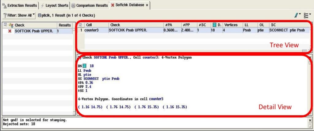
Using Calibre RVE for debugging
The Calibre RVE results viewer provides a rich set of features to facilitate efficient debugging of soft check errors. It offers detailed information on conflicting shapes, enabling designers to understand the relationship of shapes to the design. The viewer allows for easy examination of upper and lower layer connectivity and provides visualization tools for better comprehension.
Figure 4 shows the expanded detail displayed in the Calibre RVE results viewer. The tree view at top includes the following attributes:
- annotations for each result that detail the cell where the result is located
- the soft check that generated the result
- the net associated with the result
- the upper and lower layer names
- other properties of the result
Conclusion
Soft checks are indispensable for identifying and resolving connectivity issues between diffusion layers and well regions in IC design layouts. Understanding the intricacies of well layer connectivity and adopting a systematic approach to debugging soft checks are crucial for design teams. Tools like Calibre RVE give designers accurate reporting and visualization capabilities, ensuring a consistent debug flow across diverse design styles and process nodes. Accurate detection and correction of these connectivity errors contribute to the overall performance, reliability, and timely market release of IC products.
Watch Terry’s video here further discussing soft-check debugging