What’s an ESD design window, and why do I care?
By Derong Yan
As we move to advanced semiconductor process nodes, electrostatic discharge (ESD) issues have become more critical in integrated circuit (IC) chip designs. To protect IC chips from ESD damage, there are many ESD design rules and guidelines that chip designers must follow. Familiar ESD design rules include checking for the existence and size of ESD protection devices, the robustness of ESD discharge paths, and the resistance from chip-level bumps to ESD protection devices.
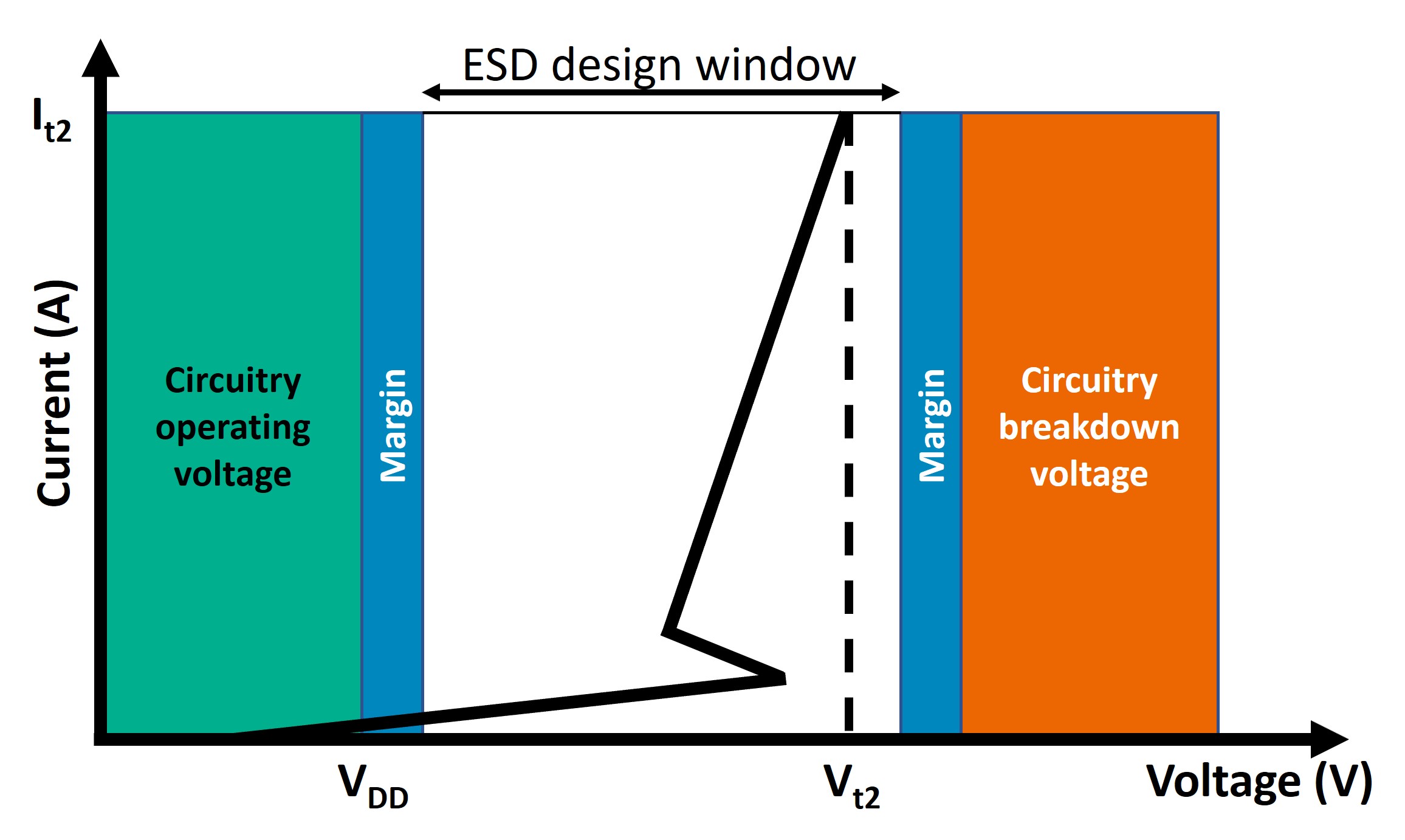
However, there is another critical aspect of correct ESD design that is often overlooked—making sure that an ESD protection device operates inside a properly-defined ESD design window. An ESD design window defines the voltage and current limits within which an ESD protection device operates during an ESD event. Designers know the circuitry operating voltage, and after selecting the type and size of an ESD protection device, they know the operating and failing voltages and electrical current limits of the ESD protection device. The missing part is the determination of the upper voltage limit of the ESD design window, which is limited by the breakdown voltage of the victim circuitry. Ideally, an ESD protection device is triggered or turned on at a voltage that is above the normal circuitry operating voltage, but will fail or break down itself before the voltage reaches the breakdown voltage of the victim circuitry.
Estimating the “best” upper voltage limit for the ESD protection device can be tricky. If the victim device (which is the device directly connected to the ESD protection device) is not directly connected to the ground, i.e., if there are several other devices connected in series between the victim device and the ground, using the breakdown voltage of the victim device alone as the breakdown voltage of the victim circuitry may be overly pessimistic. On the other hand, designers never want to overestimate the ESD protection device breakdown voltage, as this can result in the victim circuitry being damaged before the ESD protection device fails or breaks down.
Some IC chip designers do their own diligence to manually identify all possible electrical paths between the victim device and the ground, add up the breakdown voltages of all device junctions on each path, find the path with the lowest total breakdown voltage, and use this lowest total breakdown voltage as the breakdown voltage of the victim circuitry. However, in addition to being time-consuming, this approach is virtually impossible to accomplish in a complex IC chip design, which may have hundreds of possible electrical paths and millions of devices along these paths to analyze.
Fortunately, IC chip designers don’t have to rely on their eyeballs or manual methods anymore. The Calibre® PERCTM reliability verification platform can help them quickly search the netlist to identify all possible electrical paths from a victim device to the ground, and automatically find the path with the smallest total breakdown voltage. When combined with the Calibre RVETM results viewer and Calibre DESIGNrev layout viewer, the Calibre PERC platform allows IC chip designers to not only quickly estimate an appropriate breakdown voltage, but also see a visual representation of the electrical path with the lowest total breakdown voltage in schematic or layout view.
If automated calculation of breakdown voltages sounds good to you, check out our technical paper, A better way to estimate breakdown voltage for ESD design windows.