In the EDA world, efficiency + ease of use = productivity (and profitability!)

By Shelly Stalnaker
Electronic design automation (EDA) grew out of the need to make it easier and faster to design and manufacture integrated circuits. Nothing has changed since then, except…everything has changed. Just a couple of decades ago, we were entering “unknown territory”—the sub-nanometer era. Today, foundries and design companies are exploring 1nm process nodes. In all that time, the EDA industry constantly expanded functionality to address new design and manufacturing requirements, increased processing speed and flexibility to enable companies to meet their market schedules, and added new tools to help design teams build and use process flows more effectively.
The importance of the EDA infrastructure is clear when we look at the content that is catching peoples’ attention recently. How can we remove roadblocks in our design and verification flows, or prevent early design issues from becoming major obstacles during signoff? How can we standardize our processes across multiple teams, but still allow each team to choose its own path for maximum efficiency? How do we keep improving our accuracy and precision during debugging and fixing? In reality, the answers to all those questions can be summed up as…How do we get the most value from our EDA tools and functionality?
To help you answer those questions, we’ve selected some recent articles and blogs by Calibre Design authors that may point you in new directions, remove impediments that are costing your company in both time and resources, or simply make a routine process simpler and/or faster for your designers. After all, who doesn’t like it when their job suddenly gets easier?
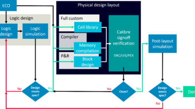
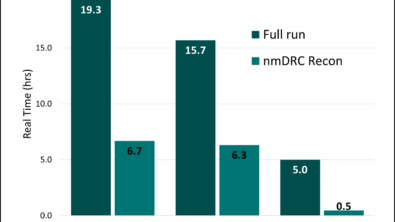
Hit your tapeout schedules with in-design signoff DRC
Using sign-off DRC inside your P&R environment can not only reduce the number of signoff DRC iterations you’ll need, but also enable you to apply early layout optimizations to meet PPA goals.
Custom layout designers…Want to know a secret? You can close DRC faster. A lot faster…
Closing custom design DRC at mature nodes can be time-consuming. In-design signoff DRC helps custom designers quickly find and fix critical DRC errors that may be gating their tapeouts.
Get rid of GUI frustration and speed up your Calibre verification job submissions!
Need a standard Calibre invocation that still allows for customization among different teams? The enhanced Calibre Interactive GUI is the interface you’re looking for.
Caution! Avoid detours when improving resistance on ESD paths
Correcting and improving the resistances of ESD discharge paths can be trickier than you think. Learn how to avoid heading in the wrong direction.
Can we just agree that perception is everything? Especially in IC design?
A standardized, yet customizable layout viewer lets companies ensure that corporate and team requirements are observed, while enabling individuals and teams to modify the interface to suit their individual preferences and needs.
Now You Can Automate Latch-Up Verification For 2.5/3D Technologies
New ways of using existing tools enable design teams to use topology-aware and voltage-aware flows to verify external and mixed-voltage latch-up design rules in 2.5/3D IC designs.
Efficient package delivery is not just for FedEx!
Successful HDAP design requires design teams to work together to optimize the entire system. Taking the time to organize and optimize your HDAP design processes is a crucial element.
Want to learn about even more ways to improve your processes and productivity? To explore the full range of our blogs and articles, be sure to visit the Calibre Design blog and follow Design with Calibre on LinkedIn. Have questions or comments? Let us know below!