All Together Now: FOWLP in the Foundry
By John Ferguson, Mentor Graphics
FOWLP design popularity is driving foundries to develop in-house FOWLP flows. How will that affect the market?

The technical challenges of implementing fan-out wafer level packaging (FOWLP) are well known by now [l].
The interplay between system-on-chip (SoC) technologies and packaging requirements requires co-validation between integrated circuit (IC) and package design environments. The choice of operating system, IC or packaging technology, manufacturing output format, netlist format—these considerations , among others, can make the decision to adopt FOWLP a difficult choice to justify. However, the very difficulty of that decision has provided a new opportunity in the FOWLP marketplace.
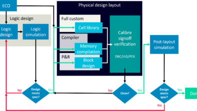
Foundries are now developing their own integrated offerings for FOWLP. With a dedicated process flow and certified tools, design companies can realize the benefits of FOWLP technology without the worry, time, and expense of assembling design, layout, and verification flows from many disparate components and tools. Additionally, the foundry can provide dedicated packaging lines for these flows, ensuring availability and consistent, uniform processing. Electronic design automation (EDA) companies are also stepping up to deliver design and verification tools that support these solutions. Mutual customers can take advantage of these offerings to design and deploy FOWLP products using proven design methodology and certified EDA tools.
Comparing a foundry FOWLP process to that available from an outsourced assembly and test (OSAT) company illustrates some of the advantages and disadvantages of each approach, as shown in Table 1. The most obvious advantage for design companies is the option to work with a single point of contact and a single process flow. Foundries have extensive expertise in generating process design kits (PDKs) for advanced IC processes. Now they are bringing that knowledge and expertise into the package co-design world. Not only do they have the advantage of significant experience and long, historic relationships with the EDA companies, they also control both the package and the die process details. This control enables them to more readily access information across the IC and package domains than might be possible when working with multiple parties.
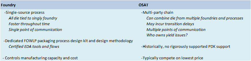
Table 1. Comparison of a foundry FOWLP process to that of an OSAT.
With respect to the above discussion, for example, it would be difficult for an outsourced semiconductor and test (OSAT) supplier to put together a generic solution to solve parasitic extraction issues where die signals and package signals affect each other, because the OSAT only has detailed knowledge about the package. Not only does it have little insight as to what might be in the dies, it may also have various legal restrictions as to what it is allowed to divulge to other IC suppliers.
By unifying the IC and package design and process flow, the foundry can ensure uniformity and consistency across designs. Troublesome features or packaging issues can be resolved more quickly, and the solutions can be implemented across all future designs. EDA tools can be enhanced or modified to address design and verification issues specific to that foundry. What that means to the designers is the ability to find and fix potential design issues earlier in the process, saving costly iterations and time-to-market.
On the other hand, having a single foundry control the FOWLP process means design companies will most likely be restricted to using dies produced by that foundry. If the goal is to unify and streamline the process, limiting die to those produced in-house is a logical choice. While this may not be an issue for some design companies, others may find it constricts their design and product options, limiting their available market opportunities. Those companies may choose to pursue or continue using an OSAT to ensure they can select from a full range of die options for their package offerings.
The availability of a dedicated PDK will be attractive to design companies, given the increased complexity associated with FOWLP design and verification. Manual control and checking of these designs is no longer practical from either a time or accuracy standpoint. In fact, some OSATS are now looking to implement their own PDKs to reduce the risk of these package designs [2].
The potentially faster throughput and availability of dedicated packaging lines may prove to be irresistible to companies for whom time-to-market is the predominant success factor. On the one hand, foundries may be incentivized to provide manufacturing capacity to customers using their internal FOWLP process, but on the other hand, they have full control of that capacity and the associated cost. OSATS traditionally compete on lowest cost, making them an attractive choice for design companies looking to control expenses. However, the overt financial costs belie many of the hidden costs discussed above, so companies must carefully consider all of their resources and options when choosing which path to pursue.
One of the first foundries to announce an in-house FOWLP process was TSMC, with its integrated fan-out (InFO) wafer-level packaging process that eliminates silicon, through-silicon vias (TSVs) and silicon interposers. The InFO process flow enables TSMC customers to deploy the unique fan out layer structures and interconnects in the InFO technology, targeting cost sensitive applications such as mobile and consumer products.
To ensure InFO design support, TSMC worked with EDA companies such as Mentor Graphics [3] to develop EDA solutions for IC and package design, including packaging design and layout, as well as physical verification. This congruency ensures that lnFO designs are fully compliant with TSMC ‘ s packaging design rules and sign-off requirements to ensure adequate yield and reliability, and enables the foundry to provide a complete InFO design flow for its customers. Through its Open Integration Platform (OIP), TSMC has already established rule deck support for co-validation between IC and package design environments, including design rule checking (DRC) verification, layout vs. schematic (LVS) comparison, and inter-die DRC/LVS. The company is currently expanding InFO tool support into electrical analysis and sign-off , including parasitic extraction (to enable designers to analyze the parasitic impacts from InFO and its neighboring layers) and multidie reliability analysis (analysis of electromigration (EM) and IR drop). In addition, TSMC and its ecosystem partners are extending the physical implementation with interdie connections, and physical s ig n-off with inter-die DRC and LVS solution s.
Intel Custom Foundry recently introduced its embedded multi-die interconnect bridge (EMIB) as a cost effective approach to in-package high density interconnect of heterogeneou s chips [4]. While not a true FOWLP design, it is a package option that eliminates the need for through silicon vias and replaces large silicon interposers with small die-to-die silicon bridges. They are also rumored to be working on a true fan-out wafer level packaging process, but no details have yet been made public.
As more foundries look to implement proprietary FOWLP flows, how will this affect the FOWLP market? Where will design companies go? While design strategies may drive decisions at first, the market is new enough to entice companies to reexamine their package design flows and possibly move to foundryprovided programs. On the other hand, OSATS may take their cue from these foundries and accelerate the development of their own standardized FOWLP flows to retain and expand their customer base. It will be interesting to watch the market dynamics as this technology becomes more widely used.
References
[1] J. Ferguson , “Not yet a fan of fan out? Why you should be!,”Chip Scale Review, May-June 2016; http://fbs.advantageinc.com/chipscale/may-jun_2016/#15/z (accessed August 25, 2016).
[2] H. Reiter, “Ideas for cooptimizing chip-package design,” 3DinCites, Sept. 10, 2015; http://www.3dincites.com/20l5/09/ideas-for-co-optimizing-chippackage-design/ (accessed August 25, 2016).
[3] “Mentor Graphics adds support for integrated fan-out (InFO) packaging techno logy at TSMC,” Mar. 14, 2016; https://www.mentor.com/pcb/news/mentor-info-packingtechnology- tsmc (accessed August 25, 2016).
[4] Intel Custom Foundry, “Embedded multi-die interconnect bridge,” Intel Corp., http://www.intel.com/content/www/us/en/foundry/emib.html (accessed August 25, 2016).
Author
John Ferguson is the Director of Marketing for Calibre DRC Applications at Mentor Graphics

Liked this article? Then try this –
Blog: Not yet a fan of fan-out? Why you should be!
This article was originally published on www.chipscalereview.com