Pattern Matching In Test and Yield Analysis
By Jonathan Muirhead and Geir Eide, Mentor Graphics
Analyzing fail data with pattern matching helps companies identify yield limiters faster to increase yield ramp

It’s no secret that a successful yield ramp directly impacts integrated circuit (IC) product cost and time-to-market. Tools and techniques that help companies ramp to volume faster, while also reducing process and design variability, can be the difference between profit and loss in a competitive market. And while pattern matching technology has been around for a while now, both foundries and design companies are finding new ways to employ it in test and yield analysis processes to improve both current and future yield ramp improvement.
During process development, foundries and design companies use a variety of test and yield analysis tools to analyze die and identify systematic failures and yield limiters that are specific to that process node (Figure 1). They can then use this knowledge to write new or enhanced design rules that help designers avoid such configurations in future designs. This “wafer learning” is a part of every new process development.
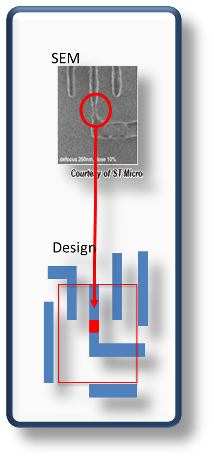
Figure 1. Identifying and analyzing systematic failures in die can help designers avoid problematic geometries.
However, the turnaround time for this wafer learning is becoming longer and longer at each new process node. Integrating pattern matching technology with test and failure analysis allows foundries and design companies to more quickly and accurately identify unique layout patterns that cause yield loss or reduce performance. Once fail data from wafer tests have been diagnosed by the foundry customer and analyzed by the foundry to identify systematic issues caused by physical design features, the foundry can use pattern matching technology to capture the applicable geometries and identify the instantiations of these “bad” patterns in the design (Figure 2). Reading the resulting database into a diagnosis tool enables the foundry to determine if a suspect overlaps one or more of the instances of the bad patterns. The foundry can then employ yield analysis tools to determine if the cause of the defect is actually the layout pattern, or if the correlation is just a coincidence.
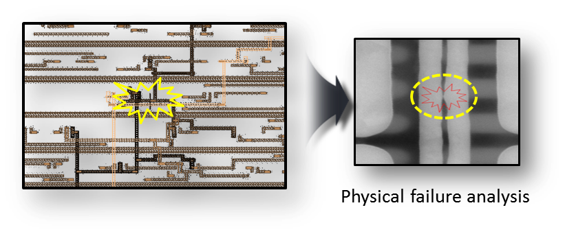
Figure 2. Physical analysis on die to identify systematic issues that affect yield.
Samsung Foundry took this approach a step further in the development of its Closed-Loop DFM solution (Figure 3) to automatically identify yield-limiting patterns, helping its customers ramp to volume faster and reduce process-design variability. Post-manufacturing, their FLARE (Failure anaLysis And yield Rank Estimation with DFM hotspot database) process uses Mentor’s Tessent Diagnosis tool for layout-aware diagnosis, the Calibre Pattern Matching solution for generating a hotspot database, and statistical analysis in the Tessent YieldInsight product to identify the yield-limiting layout patterns.

Figure 3. Samsung Foundry’s Closed-Loop DFM flow uses pattern matching in both post-manufacturing wafer analysis and pre-manufacturing design analysis to identify suspect geometries.
But it’s not just the foundry creating these patterns. Design companies are also using pattern matching in their own pre-production and test chip analysis programs to identify problematic patterns that may be unique to their designs and design methodology (Figure 4). By identifying and removing these patterns, companies can achieve faster and better yields when they go to production, a competitive advantage that can return substantial benefits in a tightly-contested marketplace.
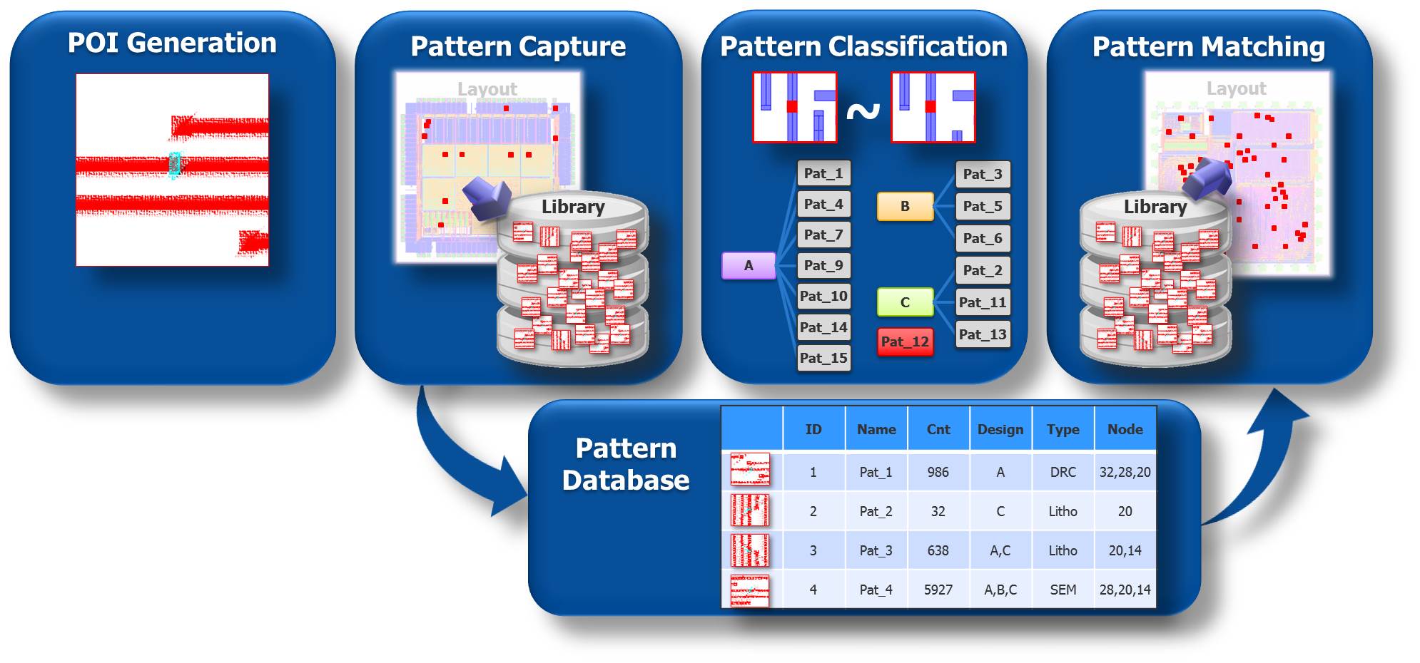
Figure 4. Pattern matching can provide a significant competitive differentiator for design companies.
Of course, as Michael White discussed previously (see link to article below), pre-manufacturing design analysis can also contribute to yield ramp improvement. By combining pattern matching with other analysis techniques, such as litho-friendly design (LFD) for hotspot recognition and design for manufacturing (DFM) for design optimization, the foundry and its customers can determine the potential impact of suspect patterns on manufacturability, and work together to make the design and/or manufacturing changes needed to ensure that the customer’s unique design style achieves target yields and reduces production ramp variability. Samsung Foundry’s PRISM (Pattern Recognition & Identity Scoring Method) is one example of how pattern matching can be combined with other design analysis techniques to analyze and categorize patterns by the severity of their impact, enabling design companies to efficiently manage design optimization.
Samsung Foundry’s experience to date has shown more than 10% product yield gains in the initial phase of production, when compared to the same design without the application of the Closed-Loop DFM system.
Pattern matching helps both foundries and design companies speed up the recognition and definition of yield limiter geometries during yield ramp for new processes and new designs. By implementing a wide variety of pattern-based yield detractor solutions in both post-manufacturing test and yield analysis, as well as pre-production design analysis, foundries and fabless companies are improving production results for today’s most complex designs at all nodes.
Authors
Jonathan Muirhead is a Product Marketing Manager for Calibre Pattern Matching in the Design to Silicon Division of Mentor Graphics.
Geir Eide is the product marketing director for the Silicon Learning product line in the Silicon Test Solutions group at Mentor Graphics. His focus is on diagnosis, yield analysis, and silicon debug.

Liked this article? Then try this –
Article: Pattern Matching in Design and Verification
This article was originally published on www.semiengineering.com


