LEF/DEF IO Ring Check Automation
By Matthew Hogan, Mentor Graphics
Designing today’s complex system-on-chips (SoCs) requires careful consideration when planning input/output (IO) pad rings…

Background
Designing today’s complex system-on-chips (SoCs) requires careful consideration when planning input/output (IO) pad rings. Intellectual property (IP) used in an SoC often comes from multiple IP vendors, and can range from digital/analog cores to IO pads, power/ground pads, termination cells, etc. Each vendor has its own rules for these IO rings to protect the IP from electrostatic discharge (ESD) and other reliability concerns. The constraints for these rules are different from one foundry to another, as well as from one technology node to another, or from one IP vendor to another (Figure 1).
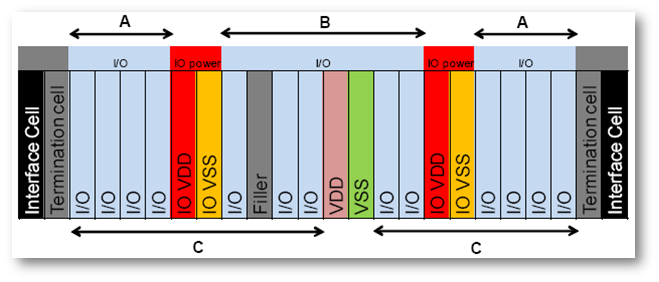
Fig. 1: Sample rule file constraints from IP supplier (1).
While detailed rules are available from each IP vendor on how to comply with their IO ring layout rules, what is not generally available are instructions for applying those rules in the presence of other IPs. Typically, SoC designers have IP from a CPU supplier and memory supplier, in addition to the IO cells. A holistic and integrated approach that allows for all of these IP pads to co-exist is needed.
Foundries provide a design rule manual (DRM) that contain guidelines for pad cell placement to protect against ESD. Typical rules found in a DRM include:
- Cell types that can or must be used in an IO ring
- Minimum number of a specified power cell per IO ring section and given power domain
- Maximum spacing between two power cells for a given power /ground pair in a power domain
- Maximum distance from the IO ring section termination (breaker cells) to every power cell
- Maximum distance from IO to closest power cells
- Cells that must be present at least once per corresponding power domain section
- Constraints for multi-row implementation
The SoC designer is then tasked with achieving the desired ESD protection across the SoC while incorporating all of the dissimilar cells and their unique rules. Needless to say, manual approaches are time-consuming, and subject to the ever-present human error factor. An automated solution that can implement the checking needed to consider all rule interactions provides a substantive improvement in both time and quality of results.
LEF/DEF IO Ring Checker
In collaboration with the I/O design group at ARM®, Mentor Graphics developed an automated framework (Figure 2) to verify SoC compliance with these foundry IO placement rules, using the Calibre® PERC™ reliability verification tool. The Calibre PERC tool can combine both the geometrical and electrical constraints of a design to perform complex checks that incorporate layout restrictions based on electrical constraints or variations.
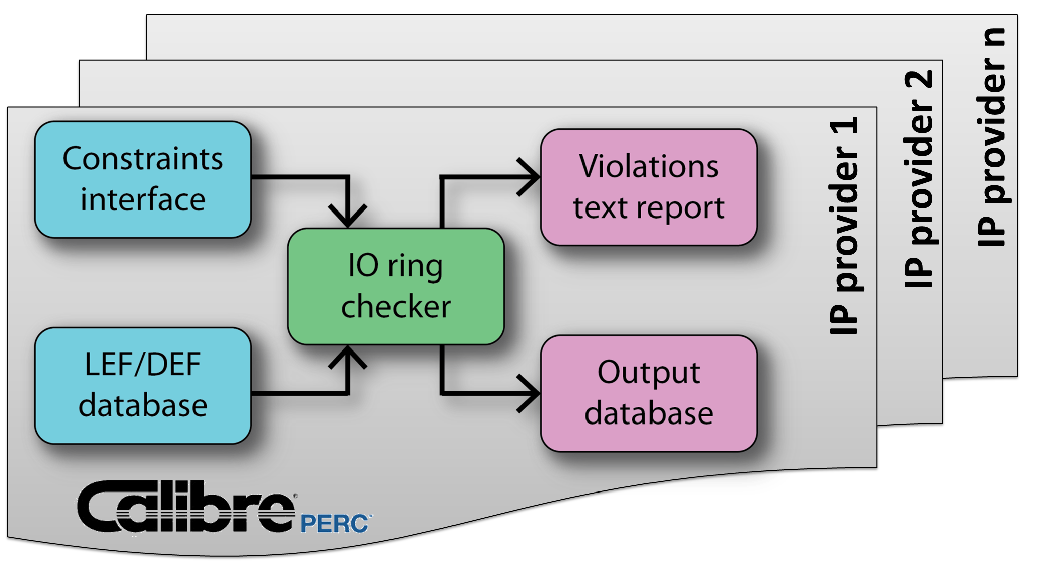
Fig. 2: Automated framework for IO ring verification.
This IO ring checker framework provides the following characteristics:
- No technology dependencies: ESD placement rules are coded in the IO ring checker, and are not constrained by or subject to any technology file dependencies.
- Easy set-up: The constraints interface (Figure 3) allows for customized cell naming conventions and spacing variables.
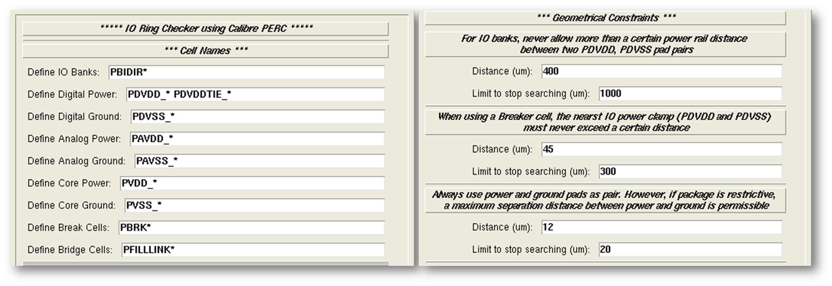
Fig. 3: The constraints interface enables easy customization.
Figure 4 shows the IO ring checker verification flow. An initial placement of IO cells is made with only IO cells in the DEF. Violations identify locations where changes to the IO ring initial placement must be made. This process continues until final placements are available. As the design nears completion, all cells and routings are now present. Another round of validation is performed until the design is complete, with all errors in IO ring placements corrected for final sign-off validation.

Fig. 4: IO ring checker verification flow.
Outputs
Two results database (RDB) files are output as part of the checking flow:
- IO_ring_checker.rdb: contains violations
- debug.rdb: contains additional information for debug
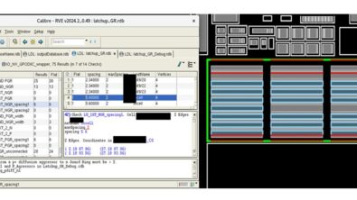
Violations can be highlighted from the IO_ring_checker.rdb file (Figure 5).
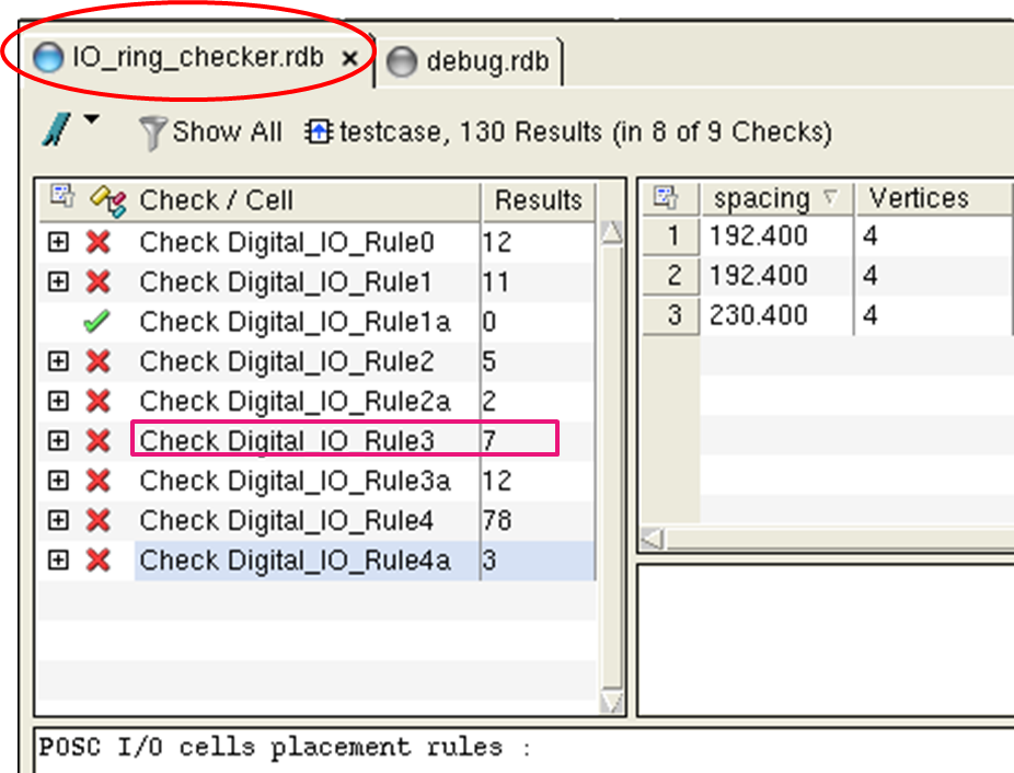
Fig. 5: The IO-ring-checker.rdb file provides quick identification of rule check violations.
If more details are required, the debug.rdb file (Figure 6) can be used to display complementary information that describes the violation more explicitly, such as:
- Cell identification (power clamp families, breakers, etc.)
- Sub-check results (for each power domain)
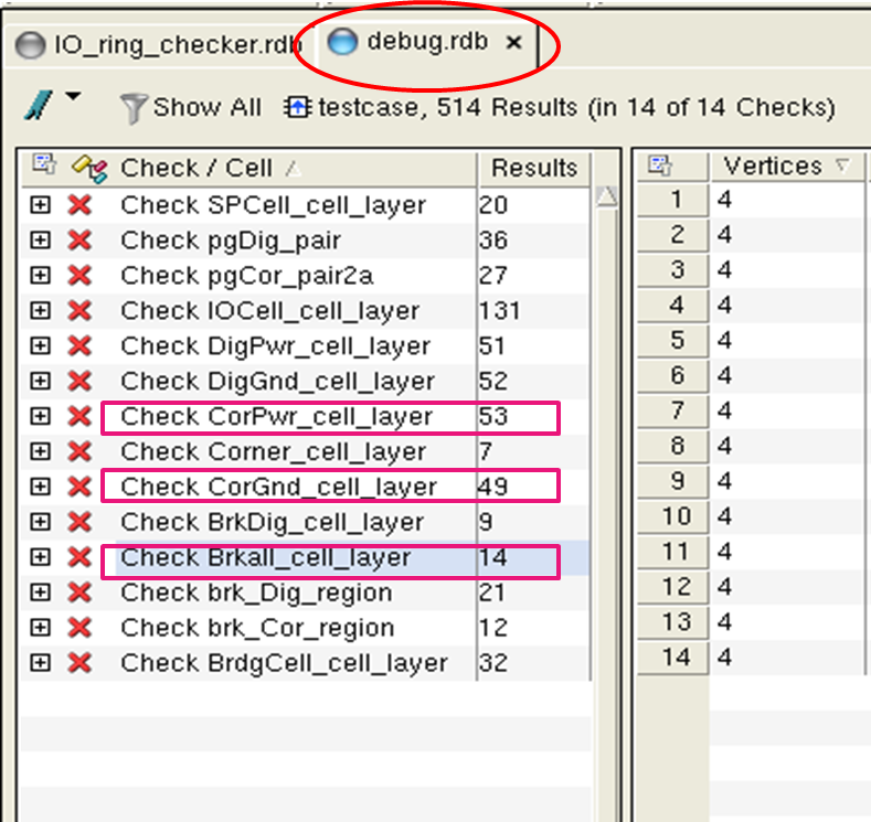
Fig. 6: The details provided in the debug.rdb file help designers understand and correct violations quickly and accurately.
For ease of use, results can be loaded and highlighted in a results viewing environment, such as the Calibre RVE tool (Figure 7), using a DEF or GDS Database. Highlighting options in the Calibre RVE tool include:
- Rule violation: IO distance to PWR/GND cells (in red)
- Cell marking: IO PWR/GND pairs (in green)
- Power domain: digital section (in blue)
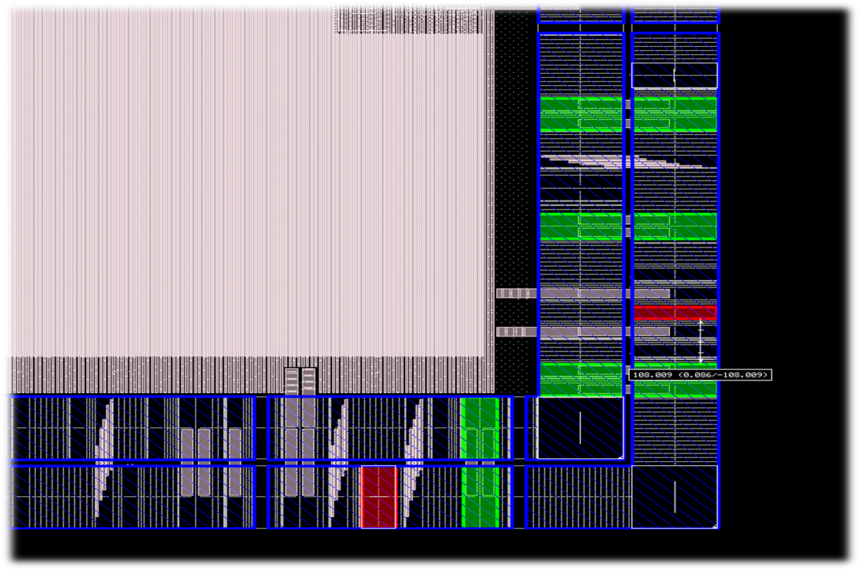
Fig. 7: A results viewing environment allows designers to visualize error results.
Results
The LED/DEF IO Ring Checker framework was applied to multiple GPIO test chips. Results demonstrate the effectiveness and speed of the framework in applying multiple rule checks across the chip (Table 1).
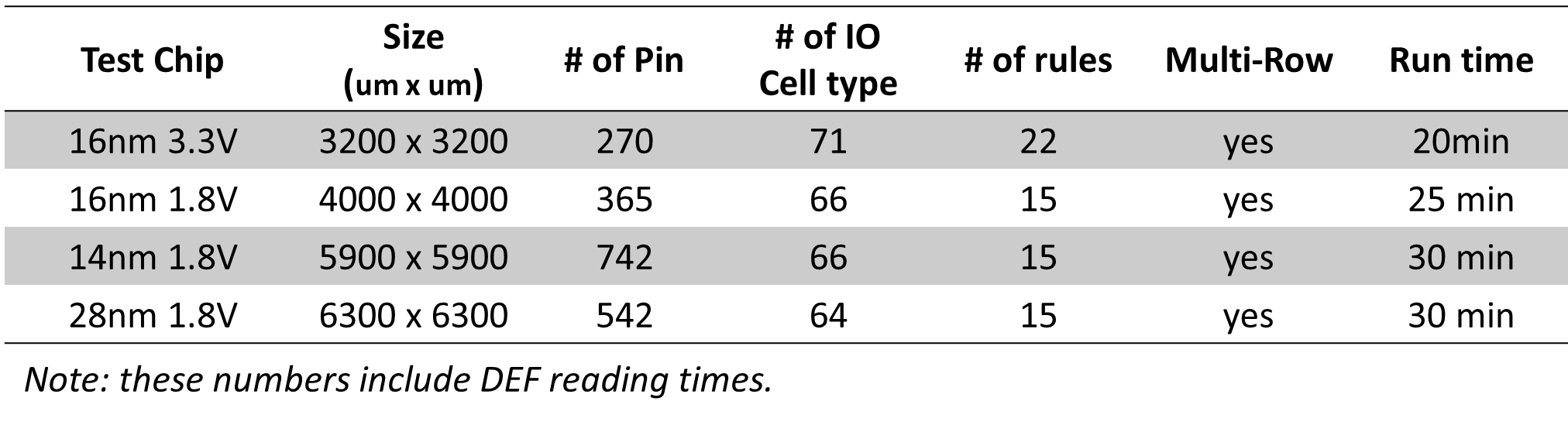
These results not only demonstrate the accuracy of this approach, but also the speed of such a solution. Manual checking could easily take days to validate, and still be error-prone. With more and more IP being implemented in SoC designs, the number of rules is only expected to grow, further complicating the verification task.
Conclusion
A flexible and automated approach to IO pad ring placement verification allows designers to focus on their design, using the IO ring checking framework and the Calibre PERC tool to confirm the validity of the layout they create. The ability to perform this validation on LEF/DEF designs allows early completion of this task in the design cycle, while there is still an opportunity to optimize and refine the design before beginning final signoff verification.
Automated approaches for advanced reliability verification issues such as IO ring checking are providing significant benefits within SoC design flows. Designers who take advantage of these techniques and tools can deliver highly reliable designs, validating them quickly and efficiently, all with greater confidence in the quality of their final products. With the complexity of IP eco-systems used within SoCs constantly on the rise, and the allure of new markets such as automotive, with its exacting reliability standards, the use of automated reliability verification for these complex interactions can only be expected to grow. Adding determinism and repeatability to your IO ring checking strategy is a strong move towards improving your reliability verification capabilities.
References
[1] EDA Tool Working Group (2014), “ESD Electronic Design Automation Checks (ESD TR18.0-01-14)”, New York: Electrostatic Discharge Association, January 2015, https://www.esda.org/standards/device-design/electronic-design-automation-eda/view/1713

Liked this article? Then try this –
Video: Customer Insights: Freescale relies on Calibre PERC for creative IC verification
White Paper: Enhancing Automotive Electronics Reliability Checking
White Paper: Reduce Verification Complexity in Low/Multi-Power Designs
This article was originally published on www.semimd.com