Design Rule Checking for Silicon Photonics
By Ruping Cao, Mentor Graphics
Verifying silicon photonics designs requires new techniques, like equation-based DRC

The silicon photonics integrated circuit (PIC) holds the promise of providing breakthrough improvements to data communications, telecommunications, supercomputing, biomedical applications, etc. [1][2][3][4]. Silicon photonics stands out as the most competitive candidate among potential technologies, due in large part to its compactness and potential low-cost, large-scale production capability leveraged by current CMOS fabrication facilities. However, as silicon PICs gain success and prospects, designers find themselves in need of an extended design rule checking (DRC) methodology that can ensure the required reliability and scalability for mass fabrication.
Traditional DRC ensures that the geometric layout of a design, as represented in GDSII or OASIS, complies with the foundry’s design rules, which guide designers to create integrated circuits (ICs) that can achieve acceptable yields. DRC compliance is the fundamental checkpoint an IC design must achieve to be accepted for fabrication in the foundry. DRC results obtained from an automated DRC tool from a trusted EDA provider are required to validate the compliance of a design with the physical constraints imposed by the technology.
However, traditional DRC uses one-dimensional measurements of features and geometries to determine rule compliance. PICs present new geometric challenges and novel device and routing designs, where non-Manhattan-like shapes—such as curves, spikes, and tapers—exist intentionally. These shapes expand the complexity of the DRC task, even to the extent that it is impossible to fully describe some physical constraints with traditional one-dimensional DRC rules.
To address the DRC challenge in photonic designs, new verification techniques are required. At Mentor, we developed the Calibre (R) eqDRC (TM) technology, an extension to the Calibre nmDRC tool. The Calibre eqDRC functionality is an equation-based set of statements that extend the capabilities of traditional DRC to allow users to analyze complex, multi-dimensional interactions that are difficult or impossible to verify using traditional DRC methods. While the development of the Calibre eqDRC functionality was originally motivated by the IC physical verification difficulty at advanced technology nodes [5], the Calibre eqDRC process is equally adept at satisfying the demand for PIC geometrical verification requirements. Users can define multi-dimensional feature measurements with flexible mathematical expressions that can be used to develop, calibrate and optimize models for design analysis and verification [6][7]. Let’s look at a couple of examples.
False Errors Induced by Curvilinear Structure
Current EDA tools support layout formats as GDSII, where geometric shapes are represented in polygons (Manhattan design). The vertices of these polygons are snapped to a grid, the size of which is specified by the technology. This mechanism produces specific DRC problems for photonic designs that include curvilinear shapes (like bends for routing) in a range of device structures, which derive from the requirement of total internal reflection for light guiding while minimizing light loss. With traditional EDA tools, the curved design layer is fragmented into sets of polygons that approximate the curvilinear shape, which results in some discrepancy from the design intent.
While this discrepancy of a few nanometers (dependent on the grid size) is negligible compared to a typical waveguide design with a width of 100 mm, its impact on DRC is significant. The tiniest geometrical discrepancy can generate false DRC errors, which can add up to a huge number, making the design nearly impossible to debug. Figure 1 shows a curved waveguide design layer, with the inset figure showing a DRC violation of minimum width. Although the waveguide is correctly designed, there is a discrepancy in width value between the design layer (off-grid) and the fragmented polygon layer (on-grid), creating a false width error. Even though these properly designed structures do not violate manufacturability requirements, they generate a significant number of false DRC errors. Debugging or manually waiving these errors is both time-consuming and prone to human error.
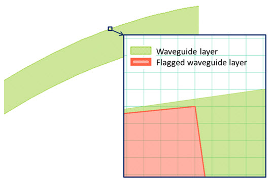
Figure 1. Design of a curved waveguide on a 1 nm grid. The enlarged view shows the polygon layer that flags the width error of the waveguide. The polygon vertices are on-grid, which results in the discrepancy in width measurement.
By taking advantage of the Calibre eqDRC capabilities, users can query various geometrical properties (including the properties of error layers), and perform further manipulations on them with user-defined mathematical expressions. Therefore, in addition to knowing whether the shape passes or fails the DRC rule, users can also determine any error amount, apply tolerance to compensate for the grid snapping effect, perform checks with property values, process the data with mathematical expressions, and so on.
Multi-dimensional rule check on taper structure
Another important photonic design feature that does not exist in IC design is the taper, or spike (any geometrical facet where the two adjacent edges are not parallel to each other), as shown in Figure 2. This kind of geometry exists intentionally, especially in the waveguide structure, where the optical mode profile is modified according to the cross-section variation (including the width from the layout view, and the depth determined by the technology).
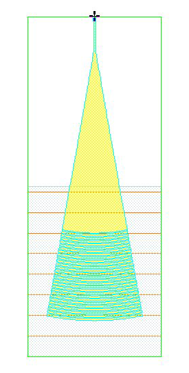
Figure 2. Tapers are a common construct in photonics designs.
The DRC check to ensure fabrication for these structures must flag those taper ends that have been thinned down too far, which can lead to breakage, and possible diffusion to other locations on the chip to create physical defects. A primitive rule to describe this constraint could be stated as:
minimum taper width should be larger than w; otherwise, if it is smaller than w, the included angle at the taper end must be larger than α.
This rule is a simple form of describing the constraint that, as the taper angle increases, the taper end width can decrease. In even simpler words, a sharper pointy end is allowed as taper end width increases. The implementation of this rule is impossible with one-dimensional traditional DRC, since more than one parameter is involved at the same time.
When using eqDRC capability, however, a multi-dimensional check can be written:
Sharp_End := angle(wg, width < w) < α
where angle stands for the DRC operation that evaluates the angle of the taper end with a width condition (smaller than w). This is a primitive check example, but it serves to show the power of the Calibre eqDRC functionality in photonics verification.
Modeled rule check on taper structure
The previous two examples primarily demonstrate the capability of the Calibre eqDRC process to manipulate property values to implement more precise rules for photonic-specific designs. As discussed, the Calibre eqDRC technique allows custom manipulation over various measurable characteristics of layout objects, offering greater flexibility in rule defining and coding. The examples imply the availability of user-defined expressions for property data manipulation, which can be enabled by an API for dynamic libraries or some other means, so that mathematical expressions are available through built-in languages such as Tcl.
However, the Calibre eqDRC process also enables complex DRC checks or yield prediction by applying user-defined models. In Figure 3, we’ll expand the taper DRC check to demonstrate eqDRC’s modeling capability.
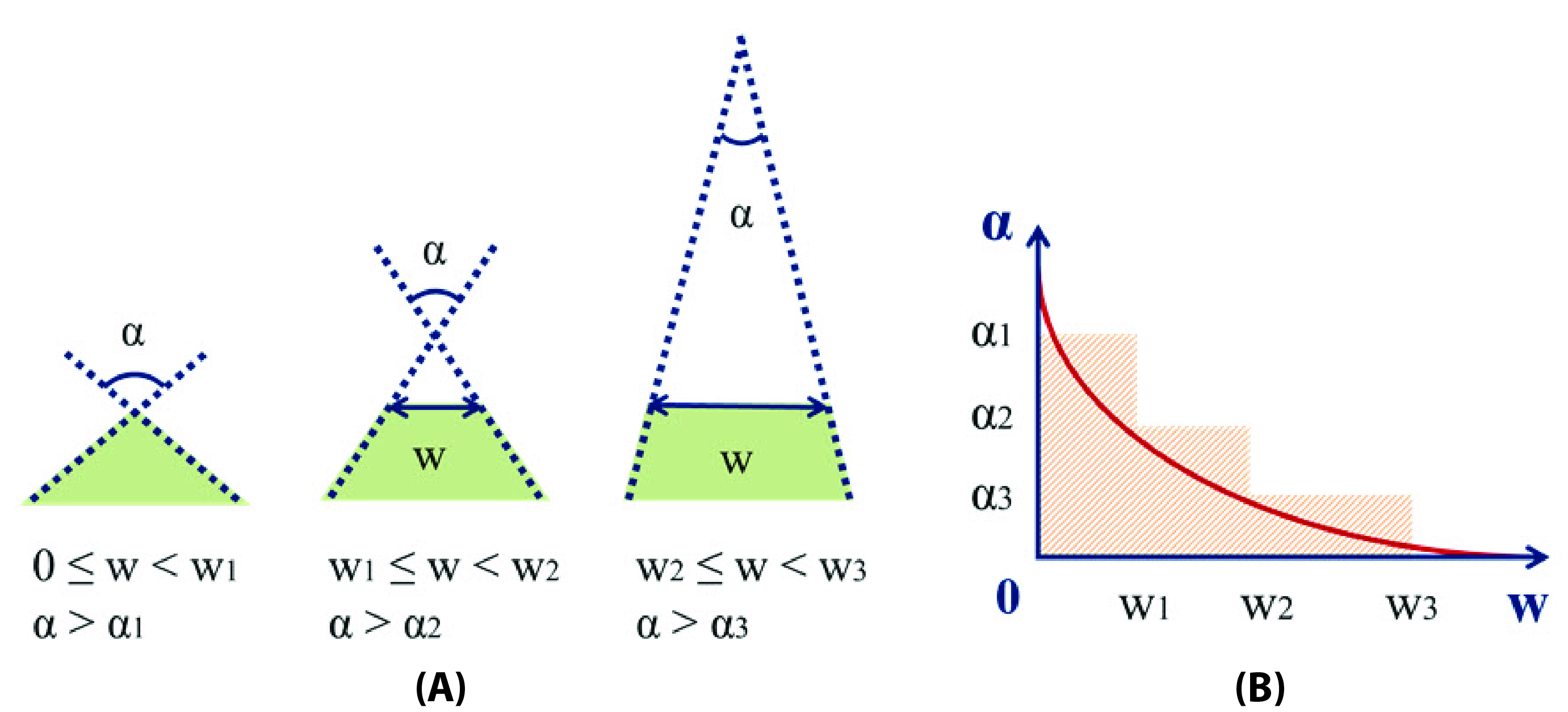
Figure 3. (A) Depiction of design rule for tapers. w is the minimum width of the taper; w1, w2 and w3 are the width values (w1 < w2 < w3); α is the including angle of the two adjacent edges of the taper end; α1, α2 and α3 are the angle values (α1 > α2 > α3). (B) Plot of rule (three separate rules are used in this case). The red line represents the modeled rule (violation happens below the curve).
Figure 3(A) depicts the rules that might be applied to those taper designs, bearing in mind that the constraint of width is correlated with the angle of the taper end. With a traditional one-dimensional rule, we can measure the critical angle value at discrete width values, and describe the fabrication constraint with three separate rules:
Rule 1: sharp_end := angle(wg, width ≥ 0, width < w1) < α1
Rule 2: sharp_end := angle(wg, width ≥ w1, width < w2) < α1
Rule 3: sharp_end := angle(wg, width ≥ w2, width < w3) < α2
Of course, additional critical angle values can be probed to add more rules to this rule set to better fit the model, but that increases the complexity of rule check tasks. So, here we have an inevitable compromise between the rule check complexity and physical constraint description integrity.
In fact, the interpolation of the critical conditions (relation of width and angle) can be expressed with a model (which should come from research and/or experimental results). Figure 2(b) depicts the constraints of width and angle given by the above rules (in shaded area). The model of critical angle against width is provided by the interpolation of the values. Here, no values are provided, and the model is only given as qualitative. The real model would require further research and proof by experimental results. Nevertheless, the example demonstrates that photonics design requires more flexible design that leads to more complex geometrical verification.
Fortunately, users can implement such models using the Calibre eqDRC capability, avoiding the dilemma of raising rule check complexity or reducing DRC accuracy. Since user-defined mathematical expressions are allowed, the relation of critical angle and width can be expressed in the rule check as follows:
sharp_ end := f(width(wg)/angle(wg) > 1
where width and angle constitute the DRC operation that evaluates the minimum width and including angle of the taper end respectively; function f is the model relating the critical angle αc and width w: αc = f(w); w is the actual measured width value. This syntax fully describes the physical constraint given by the model as depicted by the red line in Figure 2(b). In addition to being more accurate, this rule check replaces the three rule checks previously used, which simplifies the rule writing and rule check procedure.
There are several advantages to be gained by applying eqDRC to the physical verification of photonics designs.
- Ease debugging effort
Unlike traditional DRC which provides only pass and fail results, the Calibre eqDRC process produces customized information that can facilitate debugging efforts. Such information can identify the severity of the violation, suggest possible corrections, etc. This information can be displayed on the layout, helping the engineer to quickly debug and fix the violation. - Reduce false DRC errors
For photonic designs, where the existence of curvilinear shapes can lead to false errors with traditional DRC, the Calibre eqDRC method makes it possible reduce or eliminate these false errors. Because the user can apply tolerances and conditions to the check criteria, most false errors can be filtered out of the results. In addition, further investigation of remaining errors is made easier with the availability of customized information. - Enable multi-dimensional checks
Traditional DRC can measure and apply pass-fail tests in only one dimension, while the Calibre eqDRC process allows the assessment of multi-dimension parameters. Because photonic designs have a greater degree of freedom in design geometries, in many cases, multiple parameters are required to describe a physical constraint. Presently, multiple parameter analysis is only possible with the Calibre eqDRC technology. - Reduce rule coding complexity and improve accuracy
With the Calibre eqDRC process, we can apply user-defined mathematical expressions when processing layout geometry characteristics. In this way, multi-dimensional parameters that interact with each other when involved in a physical constraint can be abstracted as a model to be applied in a rule check. This not only simplifies the rule coding and rule check procedure, but also improves the accuracy of the check by replacing discrete rules with the model, which covers all combinations of parameters in one continuous function. For photonics cases where physical constraints are more complex and applied more universally, the rule coding efficiency and accuracy improvement become more important than ever. With the Calibre eqDRC approach, physical constraints can be applied closest to their design intent, and in a straightforward manner using a model description.
As photonic circuit designs allow and require a wide variety of geometrical shapes that do not exist in IC designs, traditional DRC finds it exhaustive to fulfill the requirements for reliable and consistent geometrical verification of such layouts. With the availability of property libraries to users, and the ability to interface these libraries with a programmable engine to perform mathematical calculations, the Calibre eqDRC technique offers a perfect solution for an accurate, efficient, and easy-debugging DRC approach for PICs. By finding those errors that would otherwise be missed, and flagging far fewer false errors, the Calibre eqDRC technology enables the accurate and efficient geometrical verification needed to make silicon photonics commercially viable.
References
[1] Goodman, J. W., Leonberger, F. J., & Athale, R. A. (1984). Optical interconnections for VLSI systems. Proceedings of the IEEE, 72(7), 850–866.
[2] Haurylau, M., Member, A., Chen, G., Chen, H., Zhang, J., Nelson, N. A., Member, S., et al. (2006). On-Chip Optical Interconnect Roadmap : Challenges and Critical Directions, 12(6), 1699–1705.
[3] Kash, J. A., Benner, A. F., Doany, F. E., Kuchta, D. M., Lee, B. G., Pepeljugoski, P. K., Schares, L., et al. (2010). Optical interconnects in exascale supercomputers. 2010 IEEE Photinic Society’s 23rd Annual Meeting (pp. 483–484). IEEE.
[4] Chrostowski, L., Grist, S. M., Schmidt, S., & Ratner, D. (2012). Assessing silicon photonic biosensors for home healthcare. SPIE Newsroom, 10–12.
[5] Hurat, P., & Cote, M. (2005). DFM for Manufacturers and Designers, Proc. SPIE 5992, 25th Annual BACUS Symposium on Photomask Technology (Vol. 5992, 59920G).
[6] Pikus, F. G. (2010). What is eqDRC? ACM SIGDA Newsletter, 40(2), 3–7.
[7] Pikus, F. G., Programmable Design Rule Checking. U.S. Patent Application US20090106715 A1. http://1.usa.gov/1KIYfhy
Author
Ruping Cao is a PhD student presently completing an internship with Mentor Graphics in Grenoble, France.

Liked this article? Then try this –
This article was originally published on www.semimd.com


