Deja Vu for CMP Modeling?
By Jeff Wilson, Mentor Graphics
With manufacturing innovations and new DFM solutions, CMP modeling is gaining renewed popularity

One definition of design for manufacturing (DFM) is providing knowledge about the impact of the manufacturing process on a design layout to the designers, so they can use that information to improve the robustness, reliability, or yield of their design before tapeout. Essentially, DFM is about designers taking ownership of the full “lifecycle” of a design, and going beyond the required design rule checks (DRC) to gain a competitive advantage through design optimization. One of the lesser-known DFM operations is chemical-mechanical polishing (CMP) modeling, which can identify potential CMP hotspots before tapeout.
The CMP manufacturing process is designed to improve the planarity of a design. It polishes the surface of a wafer using a combination of chemicals and mechanical pad polishing to reduce physical irregularities across the wafer. The results of a CMP process are dependent on multiple factors, including design layout, pad type, slurry composition, and the machinery that does the polishing. Since the design layout has a significant impact on planarity, the goal of the layout designer is to reduce variation as much as possible by identifying and fixing any CMP hotspots before the manufacturing team sees the design.
For example, one of the drivers for CMP modeling is the resistance impact on timing from the variation in thickness. One of the most common CMP issues is a significant difference in density as the scanner moves across the chip (known as a depth of focus, or DOF, condition). Minimizing DOF hotspots requires designers to change their floorplan or improve the way fill is done on that design.
Near the turn of the century, the development of a DFM solution that focused on identifying lithography hotspots before tapeout (litho-friendly design, or LFD) was supported by a number of foundries, and in most cases, is now a mandatory operation for the latest technology node. It appeared that CMP modeling would follow closely behind and be the next required DFM solution. At 65nm, TSMC provided a reference flow that supported CMP modeling, and to meet the expected customer demand, all three major EDA vendors invested in CMP modeling solutions.
However, advancement in CMP materials and processes, combined with enhancements to the design filling process, reduced the number of CMP hotspots organically. As a result, the value of running CMP modeling on technologies larger than 28nm was called into question, and the process never became a regular or required component of the design verification flow. Still, as technologies continue to shrink, process changes put ever-increasing pressure on the CMP process. Let’s take a look at some lessons we’ve learned, and explore why we could see a resurgence in the need for a CMP modeling solution that can improve the robustness and reliability of advanced node designs.
First, a few reasons why the CMP modeling solutions did not materialize as a required DFM solution earlier. As already mentioned, variation in resistance based on variation in thickness was validated early on as a known CMP issue. While the current qualification process at foundries requires the extraction tool to account for thickness variation, the problem is how to present this information to the designer in a useful format. A flow was developed (supported by the leading extraction tools) to provide thickness information, but it had significant limitations. At issue is how designers use thickness values in their timing flow. One of the prime challenges is that a timing analysis flow is based on best/worst case corners, but the CMP model provided a single nominal value. Until this issue is resolved, the timing impact from thickness variation is interesting, but not particular helpful to designers trying to minimize its effect by implementing design modifications.
Another factor is the advancements that have occurred in the CMP process, particularly improvements in the slurry mix. Innovations in the slurry ingredients have provided process teams with much greater control over the removal rate of the various wafer materials, which innately reduces the amount of thickness variation.
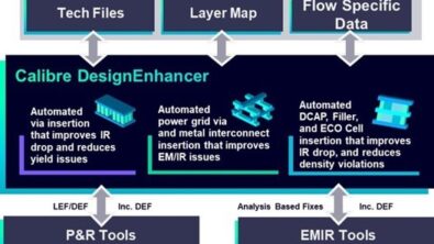
The fill process has seen similar innovations. Prior to 65 nm, the design goal was to add as little fill as possible, but the current leading technologies add as much fill as possible, using a variety of fill shapes and patterns to get as close as possible to the specified limit. While this change in fill strategy does increase the parasitic impact of fill, it significantly helps a number of manufacturing processes, including CMP. The growing importance of and complexity in requirements for the fill process led to the development of new fill tools and solutions. At Mentor Graphics, we introduced the SmartFill technology as part of our Calibre YieldEnhancer tool. The SmartFill solution combines real-time design analysis with the filling operation to provide a correct-by-construction fill solution that maximizes the placement of fill in advanced node designs. The quality of results and built-in support for new DRC requirements of the latest technologies provided by the SmartFill solution help reduce CMP variability without the need for additional design modification.
However, even though the typical ASIC or SOC designer may not see clear evidence that CMP modeling should be a required part of the design flow, there are a couple of market segments building CMP models and driving the use of CMP simulation. These companies fall primarily into two camps: 1) they produce designs that are extremely sensitive to variation in planarity, or 2) they have process teams working on the leading edge that need to reduce the impact of CMP in the latest technology nodes.
In the first group are memory and image sensors designers. Variation in planarity can have a significant impact on the yield of these designs, given the variation in density caused by the typical layout configuration. These design teams use CMP modeling capabilities from companies like Mentor Graphics to provide additional feedback on the CMP process, enabling them to identify areas of concern and make adjustments prior to tapeout to ensure they achieve the greatest design planarity possible.
The other users building CMP models are those who are pushing the technology curve. Their goal is to understand the variation that can occur with the latest technology. For example, the introduction of high-k metal gate (HKMG) technology expanded interest in the CMP process beyond the traditional shallow trench isolation (STI) and the back end of line (BEOL) fill layers to include modeling for the front end of line (FEOL) layers. A difference of a few atomic layers can lead to a measurable variability in the performance of transistors. To further complicate the matter, additional manufacturing steps are now required for the FEOL, including poly open planarization (POP) and replacement metal gate (RMG). Adding recognition of these steps to a CMP model allows designers to account for the impact of these steps during the design and verification flow, enabling them to provide better designs and improve yield.
Another process area that is gaining new attention from the process teams is the shrinking tolerance for depth of focus and its impact on the lithography process. Determining the impact of CMP on the lithography process is an interesting interaction point between these two important processing steps. We believe it is not a matter of if this interaction is going to be important, but when, and Mentor is using its experience in building models for both areas to monitor the situation and anticipate the need for new solutions.
In the EDA industry, it is always somewhat of a betting game to provide the right technology at the right time. While our early efforts in CMP modeling were successfully implemented by a select group of users, we did not see the widespread adoption we expected at the turn of the century. However, new process steps and new technologies (such as nanotubes) continuously emerge to put new pressures on planarity improvement. It could be déjà vu all over again, with CMP modeling becoming a critical component of design success.
Author
Jeff Wilson is a DFM product marketing manager in the Calibre organization at Mentor Graphics.

Liked this article? Then try this-
Video: DFM Solutions for 14nm: Samsung and Mentor Graphics
This article was originally published on www.semiengineering.com