Accurate Lithography Simulation for Silicon Photonics
By Joe Kwan, Mentor Graphics
Precise curved geometries are vital to making silicon photonics technology work
Introducing silicon photonics
A photonic IC (PIC) is a device that integrates multiple functions. The best-known example of a PIC is a fiber-optic communications system where data is transmitted through light waves rather than electrical signals. Unlike an electronic IC where the primary device is the transistor, there is no single dominant device in a PIC. The range found on a PIC can include waveguides, power splitters, optical amplifiers, optical modulators, filters, and more.
Most commercial PICs use materials like indium phosphide and lithium niobate. However, silicon photonics uses standard CMOS technology to create PICs. Silicon dioxide-based PICs aim to exploit several potential benefits: The most significant are high-speed data transfer within a silicon die, low-cost manufacturing, and high yield. CMOS processes are much more economical than those PICs have commonly used hitherto because they leverage mature manufacturing technologies and allow fabrication on advanced 8- and 12-inch wafers. Additional processing may be needed for the photonics components themselves, but there is generally no need for extra capital investment.
CMOS also gives designers the opportunity to incorporate optical and electrical signals in the same device. Silicon photonics then provides two further key advantages:
- Low power consumption (particularly compared with copper-based solutions that are expensive and entail high electrical consumption);
- Reliability (especially important for data centers, where a typical rack server’s lifespan is two years).
So, who’s using silicon photonics today, and how?
- Intel has an advanced circuits and technology integration project where an optical connection is used to replace an electrical interconnect for chip-to-chip communication. The bandwidth is expected to be 200 Gb/s to 1 Tb/s [1]; by comparison, conventional PCI-E data cables carry data at up to 8 Gb/s, while networking cables reach 40 Gb/s.
- Kotura announced an Optical Engine in 2013 that is capable of data rates of 100 Gb/s through the use of wavelength division multiplexing. This allows multiple data signals at different wavelengths to share the same optical pathways. Such devices are well suited to data-center and high-performance computing (HPC) applications where standard copper-based Ethernet networking is inadequate [2].
- The Center for Nano- and Biophotonics at Ghent University in Belgium is using silicon photonics technology to create implantable medical monitoring, diagnostic and detection devices, including a blood glucose meter with an on-chip spectrometer [3].
The trouble with the curve
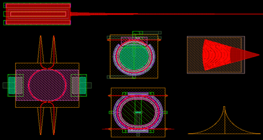
Viable silicon photonics devices require precisely drawn and characterized curved structures to ensure that the circuit performs as expected for the given wavelength of light that connects the photonic devices (Figure 1). These curved structures differ radically from the Manhattan geometries of electronic circuitry that have been the sole focus of EDA tools until now. This need to deal accurately with curves is one of the most pervasive requirements facing the adaptation of EDA design and verification tools, as well as foundry processes, to the production of silicon photonic devices.
Figure 1 Photonics devices differ from electronic devices in their use of precise curves to manipulate lightwaves (Source: Mentor Graphics)
There has already been a great deal of research into how verification processes – such as design rule checking and layout vs. schematic comparison – can be adapted to silicon photonics [4,5,6]. But what you ultimately get in silicon is still subject to manufacturing variations inherent in the lithography process. What you have drawn, characterized, and even simulated in the verification tools may be very different from what is actually created on the wafer.
Lithographic readiness for silicon photonics
Because photonics circuits are extremely sensitive to the exact shapes of devices and waveguides implemented in silicon, lithographic variations must be minimized and accounted for when projecting the behavior of a photonics system. Lithography simulation and hotspot detection capabilities in tools such as Calibre LFD are being extended in collaboration with foundries to ensure that silicon photonics designs can be faithfully reproduced on a wafer within the margins required for the performance specifications.
Calibre LFD uses a design kit provided by a foundry to enable designers to run simulations and obtain an accurate description of how a layout will perform under a specific lithographic process. By identifying lithographic hotspots (areas where the potential variation exceeds a preset boundary) before tapeout, designers can modify the design to eliminate production failures. Let’s look at some examples.
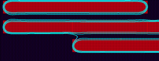
In silicon photonics, lithographic simulation must accurately predict the curves that will be in the manufactured photonics devices. Designers can achieve this by running lithographic simulation on multiple process windows to capture the ‘as-manufactured’ dimensions of the design (Figure 2). This simulation allows them to determine if the dimensions are within requirements, and if the manufacturing variance is within an acceptable range. Addressing these issues during design allows for correction before manufacturing.
Figure 2 The contours represent the simulated fabricated device. The three curves represent anticipated process variation (Source: Lukas Chrostowski, University of British Columbia)
The parameters associated with the ‘as manufactured’ simulation results can also be captured and passed back, in the form of device parameters in SPICE, to optical simulation. They are then used to determine the performance impacts of variations in the manufacturing process. Figure 3 shows a device that has been designed with 40nm square corrugations. Using the lithographic simulation of the device in a 3D Maxwell solver tool like Lumerical’s FDTD Solutions, designers can determine if the performance of the simulated device will meet the performance expectations for the manufactured device.
Figure 3 Using lithographic simulation, you can predict ‘as manufactured’ performance (Source: Wang et al [7])
While silicon photonics devices are not yet a common part of CMOS designs, the promise and potential of these systems to revolutionize high-performance and data-heavy applications is becoming ever clearer. By ensuring that EDA tools such as lithography simulators are ready and capable of providing the same level of accuracy available to electronic designs, the EDA industry is already helping to ensure that the benefits of silicon photonics are realized sooner rather than later.
References
[1] McGrath, Dylan, ‘Intel is developing optical chip-to-chip interconnects’, Electronic Engineering Times, vol. 1556, p. 39, 2009. http://www.eetimes.com/document.asp?doc_id=1170354
[2] Bigelow, Stephen, ‘Understanding silicon photonics technology’, Modern Infrastructure, vol. 2, No. 6, June 2013. http://searchdatacenter.techtarget.com/ezine/Modern-Infrastructure/Understanding-infrastructure-and-platform-as-a-service
[3] Center for Nano- and Biophotonics at Ghent University, Integrated photonic systems for mid-infrared biospectroscopy, http://www.ugent.be/nb-photonics/en/research/driver-4
[4] White, Michael, ‘Silicon Photonics Bring New Capabilities to IC Design’, Electronic Design, March 17, 2014, http://electronicdesign.com/eda/silicon-photonics-bring-new-capabilities-ic-design
[5] Unified Design Flow for Silicon Photonics, Lumerical, Unified Design Flow for Silicon Photonics, https://www.lumerical.com/tcad-products/interconnect/pyxis_eda/
[6] Ferguson, John and Cone, Chris, “Building an “EDA” Environment for Silicon Photonics”, http://bit.ly/1wFyGto
[7] Xu Wang, Wei Shi, Michael Hochberg, Kostas Adam, Ellen Schelew, Jeff F. Young, Nicolas A. F. Jaeger, and Lukas Chrostowski, ‘Lithography simulation for the fabrication of silicon photonic devices with deep-ultraviolet lithography’, IEEE International Conference on Group IV Photonics (GFP), 2012, San Diego, California, pp.288-290.
Author
Joe Kwan is Product Marketing Manager for Calibre LFD and Calibre DFM Services at Mentor Graphics.
This article was originally published on www.techdesignforums.com


