Are multi-patterning corners for parasitic extraction really necessary for 16/14 nm?
By Karen Chow, Mentor Graphics
How does multi-patterning impact parasitic extraction? How many corners do you really need?

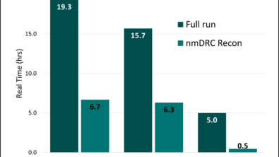
Now that 16 and 14 nm technologies are coming online, and many semiconductor companies are starting new chip design projects at those nodes, one question that keeps popping up is whether multi-patterning corners are really necessary. The post-layout simulation is frequently a big bottleneck for the verification process, and the more corners that are required, the bigger that bottleneck becomes (Figure 1).
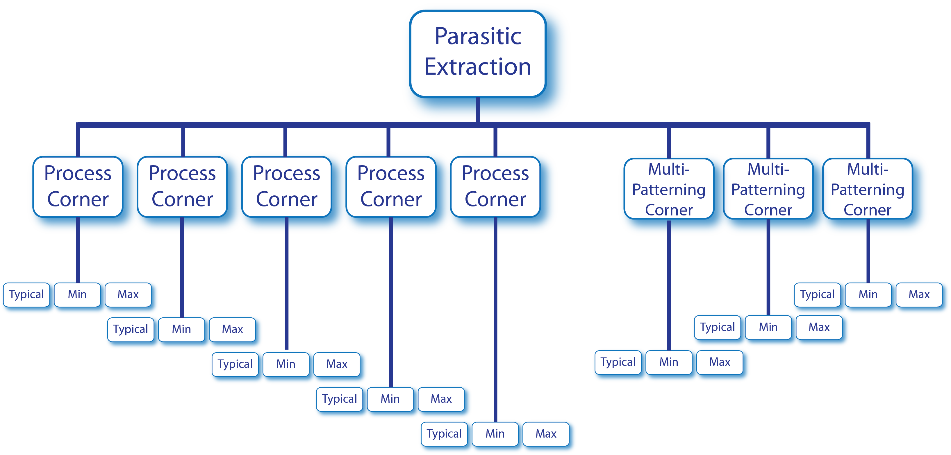
Figure 1. How many corners are really necessary for chips with multi-patterning?
What is the Impact of Multi-Patterning on Extraction?
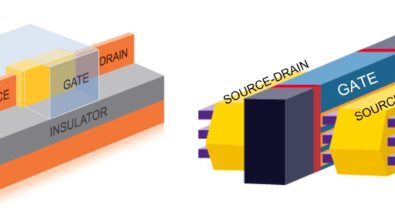
Multi-patterning is the technique required for printing geometries that are smaller than the wavelength of light used in manufacturing can accurately resolve. This is typically limited by both the lenses used and the light sources. To overcome this limitation, polygons on each layer (e.g., metal 1 layer) are split between two or more different masks, as denoted by color assignments (coloring). Printing polygons using multiple masks makes it possible to print smaller geometries than can be printed with just one mask. However, one of the drawbacks of using multi-patterning is that it is difficult to precisely align the masks. Any misalignment has an impact on parasitic capacitance, since some wires will be closer together than they should be, causing higher coupling capacitance, whereas other wires will be farther apart, thereby decreasing coupling capacitance. For example, a 6 nm misalignment causes a 15% error in coupling capacitance and a 5% error on total capacitance, whereas a 2 nm displacement creates approximately a 5% error for coupling capacitance and 2% error for total capacitance [1]. Foundries try to control this mask misalignment as much as possible, but there will always be some misalignment. Therefore, it is important to characterize the misalignment by doing simulations with the multi-patterning corners, and making sure that the circuit is robust enough to handle the resulting variation.
Colored vs. Non-Colored Parasitic Extraction
The parasitic extraction flow to capture multi-patterning effects differs depending on whether or not the layout has already been decomposed into different masks. When deciding on a multi-patterning flow, one major consideration is
whether the designer will decompose the layout into the different masks, or whether that step will happen at the foundry. Different foundries allow different levels of control by their customers for decomposing a layout into multiple masks. Some foundries only require that designs pass multi-patterning space and cycle rule checks, then do the actual decomposition themselves. Other foundries allow customers to tag certain geometries to assign them to a specific mask (a process called anchoring), or even allow customers to fully decompose their designs before tapeout.
If the foundry will do the decomposition themselves, the layout will be colorless, and the parasitic extraction methodology will not have specific information about how polygons are shifted, since the mask assignments are not yet known. In this case, corners can be used to simulate worst-case and best-case capacitance values. For colorless layouts, it is possible to change the dielectric constant to mimic geometric shifts, which assumes that all neighboring polygons are on opposite masks.
One benefit of using dielectric constant change to mimic physical shifts is that the layout polygons themselves do not actually need to be shifted, saving processing time. However, this approach is less accurate than actually calculating the polygon offset, and calculating the real change in capacitance value.
For partially-colored or fully-colored designs, designers can perform more accurate extraction, since there is knowledge about which polygons are assigned to the same mask. For this reason, some design companies want to control the decomposition process, because they want to be able to deterministically model any variance that results from the decomposition. If two polygons are on the same mask, then there will be no misalignment between them, and the corners do not need to be applied. This gives a more realistic and less pessimistic simulation result, which should allow designers to more aggressively design and lay out their circuits.
Processing More Corners
One implication of taking multi-patterning into account is that there are more corners. There are already a large number of process corners, and adding minimum and maximum multi-patterning corners for each process corner triples the corner count. This increases both the parasitic extraction time and, more significantly, the simulation runtime. Since simulation is the bottleneck of most flows, it is best to extract fewer corners during the iterative part of the design cycle, saving the extraction and simulation of all process and multi-patterning corners for signoff.
Generating Multi-Patterning Netlists
Using a parasitic extraction tool like Calibre xACT, which is designed for 16/14 nm and below, multi-patterning netlists can be generated if the rule deck provided by the foundry contains multi-patterning corners. When using Calibre xACT for digital flows, extracting three multi-patterning corners vs. one incurs only a nominal increase in runtime. During parasitic extraction, Calibre xACT can automatically output either three individual SPEF netlists, or a 3-value SPEF netlist, which is generally preferred for statistical timing analysis (STA) of multiple MP corners:
- netlist_typical
- netlist_DPworst
- netlist_DPbest
Each of these conditions has slightly different coupling capacitance values that represent the amount of mask misalignment that is possible. These three different output netlist values can now be simulated, and if the simulation results show that a certain corner no longer meets specifications, the design layout can be adjusted to make it more robust against multi-patterning misalignment. Because there is minimal overhead associated with the production of this
additional SPEF data for multiple MP corners, designers can at least determine whether or not their assumptions about the low impact of MP on STA results are correct.
Are Multi-Patterning Corners Needed for 16/14 nm?
Are multi-patterning corners needed for 16/14 nm? Unfortunately, the answer is, it depends.
Customers choose which metal scheme is best suited to their design needs. Most commonly, the M1 layer and the thin Mx layers require multi-patterning. For certain types of designs, like embedded SRAMs or standard cell designs, multi-patterning analysis will definitely be required, since much of the routing will be on the dense layers that require multi-patterning. Only by extracting both multi-patterning and process corners can these designs be made robust enough to handle potential misalignment issues and capacitance variation.
On the other hand, if digital designers only route non-multi-patterning layers, and do not perform extraction of the standard cells (since the effects are a part of the pre-included library), then it is not important to do multi-patterning corner extraction.
Understanding the implications of multi-patterning and its effects on parasitic extraction will help designers determine the best extraction approach for their designs. Employing parasitic extraction tools that incorporate automated multi-patterning corner processing can help design teams reduce the runtime impact when multi-patterning corners are required.
Author
Karen Chow is a Technical Marketing Engineer in the Design-to-Silicon division of Mentor Graphics Corp. in Wilsonville, Oregon, focusing on driving parasitic extraction development in analog and RF design flows. Prior to joining Mentor Graphics, Karen worked in the telecommunications and EDA industries, designing analog ICs and supporting EDA tool development. She received her Bachelor of Science degree in electrical engineering from the University of Calgary, and her MBA from Marylhurst University. Karen can be reached at karen_chow@mentor.com.
References
[1] Dusan Petranovic; James Falbo; Nur Kurt-Karsilayan; Double patterning: solutions in parasitic extraction. Proc. SPIE 8684, Design for Manufacturability through Design-Process Integration VII, 86840M (March 29, 2013); doi:10.1117/12.2010838.
This article was originally published on www.eetimes.com