The next chapter for PCIe: Chiplet integration with UCIe
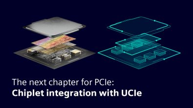
From processors and accelerators to storage, networking, and memory subsystems, PCI Express (PCIe) has been the backbone of modern compute platforms due to its high bandwidth, software compatibility, ecosystem maturity, and proven interoperability.
But as the semiconductor industry moves from monolithic SoCs to chiplet-based architectures, PCIe implementation is changing.
Traditional PCIe was designed with board-level communication in mind, where longer channels, connectors, and off-package signaling govern the physical layer. With chiplet systems, multiple dies inside the same package need to communicate over extremely short, high-density links with low latency and strong power efficiency.
Enter Universal Chiplet Interconnect Express (UCIe) 3.0. By carrying PCIe 8.0 traffic over UCIe 3.0, the PCIe protocol model and software ecosystem stay preserved over a standardized die-to-die interconnect, optimized for in-package communication. In short, PCIe keeps what made it successful, while UCIe adapts it for the chiplet era.
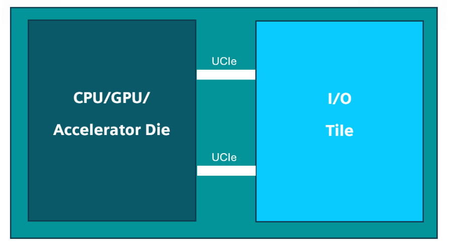
Figure 1. Package composed of CPU/GPU/accelerator die connected to I/O tile through UCIe.
Why PCIe over UCIe is the way forward
Chiplet architectures allow functions that once resided on a single die to be partitioned across multiple dies in the same package. This improves scalability, flexibility, manufacturing yield, and process-node optimization. Compute-intensive chiplets can use advanced process nodes, while PCIe or I/O subsystems can remain on more cost-efficient nodes.
The benefits are significant. Designers can disaggregate PCIe subsystems across dies, reuse IP more easily, and optimize each die for the most appropriate process node. This approach also enables more flexible product architectures, improved IP reuse, better process-node optimization, and scalable bandwidth across dies.
For AI, HPC, storage, and heterogeneous compute systems, this combination offers a practical path to scale performance while maintaining standards-based interoperability.
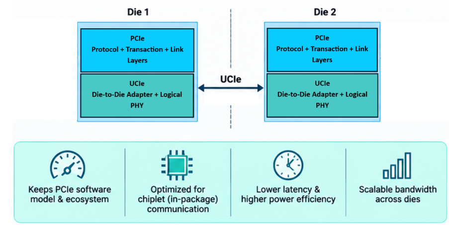
Figure 2. PCIe over UCIe – Preserving PCIe over die-to-die interconnects.
Where integration gets complicated
While the architecture is powerful, PCIe over UCIe introduces a new class of integration challenges.
PCIe has its own link training, power management, reset, recovery, ordering, credit, and retry semantics. UCIe brings its own adapter behavior, sideband coordination, mainband transport, logical PHY operation, and die-to-die link management. These layers must work together as one coordinated system for their interaction to remain coherent and meaningful.
If this coordination malfunctions, subtle failures can escalate into serious protocol violations. For example, PCIe may believe a link is active before UCIe completes reset exit and may expect traffic to flow normally across the link. A reset may clear protocol state without restoring credits and retry buffers, or a retrain sequence may fail to resume stalled traffic. These issues often appear only during full system-level verification rather than during isolated, block-level testing.
High-risk implementation gaps may remain undiscovered unless flagged by PCIe completion timeouts; these errors include lost or corrupted transactions, ordering violations, deadlocks, incorrect retry behavior, or race conditions during sideband coordination. Hence, verifying PCIe and UCIe independently is not enough. Teams must validate that PCIe transactions remain intact, ordered, recoverable, and protocol-compliant as they traverse the UCIe die-to-die infrastructure.
Smarter verification with Siemens Avery Verification IP (VIP)
Siemens Avery™ PCIe VIP and Avery UCIe VIP provide an industry-ready comprehensive framework for validating PCIe-over-UCIe designs across the complete chiplet path. Together, they allow verification teams to exercise complete cross-layer scenarios involving power management, reset, retraining, recovery, degraded-link operation, and link-error handling.
Teams can verify that PCIe traffic is correctly stalled, flushed, retried, resumed, or aborted depending on the state of the UCIe link. Siemens Avery PCIe VIP and Avery UCIe VIP also provide a comprehensive compliance test suite, with exhaustive scenarios to validate end-to-end transaction ordering, payload integrity, credit restoration, and retry-buffer behavior across chiplet boundaries.
To quickly locate the origins of failure, Siemens Avery PCIe VIP and Avery UCIe VIP provide transaction recording and protocol-aware monitors. This helps teams trace bugs anywhere across the PCIe-UCIe stack. For example, verification teams can follow a PCIe-side payload as it is packetized into UCIe flits, transported across the die-to-die link, and reconstructed on the receiving side. This makes it easier to isolate whether an issue comes from protocol handling, translation, transport, timing, or receive-side reconstruction.
Siemens Avery also offers Questa™ One Verification IQ (VIQ), an AI-driven coverage analysis solution that can quickly analyze functional coverage gaps and generate detailed insights to help accelerate verification closure.
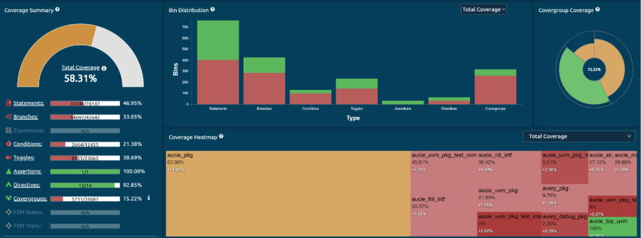
Figure 3. Functional coverage gaps highlighted by VIQ.
Building confidence in PCIe-over-UCIe systems
PCIe 8.0 over UCIe 3.0 allows designers to bring one of the industry’s most established I/O protocols into the chiplet era and disaggregate silicon without abandoning PCIe’s software model, interoperability, and ecosystem maturity. But the PCIe-UCIe boundary is where many of the hardest bugs can hide — and where confidence must be earned.
Siemens Avery PCIe VIP and Avery UCIe VIP help teams build confidence by enabling comprehensive verification across both standards and, critically, across the interaction between them. With protocol-aware models, compliance suites, randomized testing, error injection, scoreboards, and cross-layer debug visibility, verification teams can accelerate closure and reduce risk before silicon bring-up.
As chiplet-based AI, HPC, storage, and heterogeneous compute platforms continue to scale, Siemens Avery PCIe VIP and Avery UCIe VIP pave the way for high-performance PCIe over UCIe integration across chiplet boundaries.
For a deeper dive into the full verification architecture, download the complete whitepaper:
PCIe 8.0 over UCIe 3.0: Bringing a Proven Protocol into the Chiplet Era.