DFT and the competitive edge

Smart DFT for quality and TTM
Don’t let your plans for successful new SoCs be derailed by a lack of a good DFT tool infrastructure.
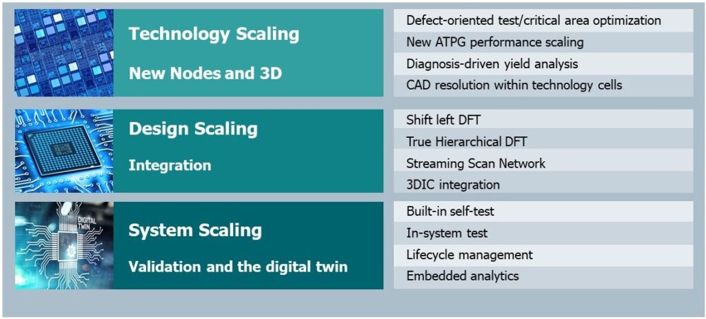
Semiconductor companies have to continually refine and optimize all aspects of chip design and fabrication in order to stay competitive as complexity increases. We recognize the drivers of SoC complexity as technology scaling, design scaling, and system scaling. Each introduces challenges through the design, manufacturing, and functional operation phases of a device. Addressing technology scaling requires tools with higher precision than before; managing design scaling requires simplification in the DFT flow; system scaling calls for in-life monitoring and analysis.
The tools and methodologies a design team chooses can make a real difference in the success of a project. Not least among the concerns is design-for-test (DFT), which includes a broad range of test-related design tasks, from insertion and verification of test logic during RTL design and continuing all the way to failure analysis of field returns and in-life monitoring of performance, faults, and security. Simply adding scan compression and creating traditional test patterns is no longer a recipe for success.
Tessent, as the market leader in DFT, yield improvement, and in-life test, works closely with the leading companies throughout the semiconductor ecosystem to create the advanced DFT tools and methodologies that ensure success for our customers. Whether the goal is meeting ISO 26262 functional safety requirements, improving yield, reducing cost, or meeting the design deadline, Tessent software and IP simplifies DFT in a way that significantly improves time-to-market without sacrificing test quality.
To learn more about the elements of an advanced, smart DFT strategy and know how to go about building the best DFT for your needs, read our technical paper “How to maximize your competitiveness in the semiconductor industry using advanced DFT.”
The paper outlines the significant areas of research and development focused on solving DFT and yield challenges for today’s designs. No matter what the specific DFT needs are for your design, there are some basic requirements for a DFT solution, including:
- It uses the most effective techniques for detecting manufacturing defects
- It integrates efficiently into various common design flows and functional system requirements
- It can leverage DFT and production test results to improve yield, which directly impacts both time-to-volume and profitability
Find the defects, fast
The primary directive of DFT is to catch defects in manufactured silicon and ensure that a part is defect-free before it’s placed in-system. Also, it shouldn’t take too long. The specifics of each of those directives changes with each design.
For example, some ICs require a ‘near-zero defect’ quality. These designs will likely need to use cell-aware fault models that can target potential defects within the technology cells. Cell-Aware ATPG is in use at major semiconductor companies, who reported dramatic improvements in fault coverage. ATPG advances include new types of bridge, opens, cell-aware/timing-aware, and cell-neighborhood tests. These so-called “defect-oriented” test has been vetted by the likes of Intel and ON Semiconductor in published research papers (Howell, 2018 & Maxwell, 2017).
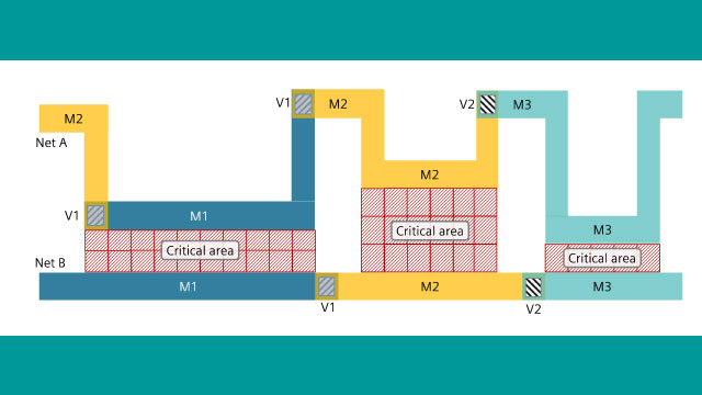
Tessent also improves test coverage while decreasing the test pattern counts by using critical-area layout information to select and order the most effective test patterns. The approach uses the total critical area (TCA) associated with faults detected by a pattern. In other words, we first determine the likelihood of defects occurring based on their critical area, then we can sort the various pattern sets considering the defects they detect to choose the most effective patterns to apply. The result is better coverage with fewer patterns, which translates to lower cost and faster test.
To reduce the need for more compute resources and tester capacity, we introduced a new kind of test point that dramatically reduces pattern sizes. Companies like Broadcom have used these new test points to control the growth of test pattern counts. An even newer technology for logic built-in-self-test (BIST), called LBIST Observation Scan Technology (LBIST-OST), was designed specifically to improve in-system test speed for automotive devices. LBIST-OST was awarded the 2020 Elektra Design Tools and Development Software Award from a crowded field of nominated technologies for its ability to help automotive ICs meet functional safety requirements while keeping pattern count manageable.
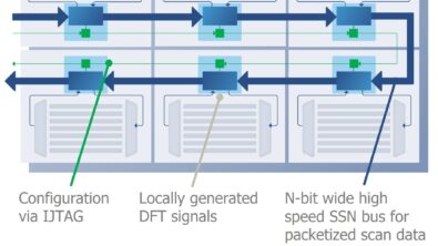
The latest Tessent offering to speed up test is called Streaming Scan Network (SSN). It is the first commercial DFT technology to use bus-based packetized scan data delivery. SSN greatly simplifies and automated DFT optimization in a scalable and flexible way. It reduces test time through high-speed data distribution, efficiently handling imbalances between cores, and by supporting testing of any number of identical cores with a constant cost. It provides a plug-and-play interface in each core that is well suited for abutted tiles, and simplifies scan timing closure. It is being quickly adopted by the industry because it reliably cuts DFT time in half, reduces test time by up to 4X, and is silicon-proven.
Improve the yield
Tessent software can improve the manufacturing process and increase yield, which has a direct impact on business success. Data from failed manufacturing tests can reveal valuable information about the mechanisms that cause the circuit to fail. Analyzing this data using scan diagnosis significantly speeds to time to find root causes of failure. Advanced scan diagnosis has been used by leading foundries to find root causes of failures more efficiently.
The aggregate data from a whole population of failing die across wafers and lots helps fix systematic yield problems that eat into profit. This volume scan diagnosis, an advanced technique that uses statistics and machine learning, is in use in many successful companies.
Streamline the DFT flow
Any single Tessent DFT or yield tool alone won’t necessarily lead to the time and cost savings that chip companies need to be competitive. Your set of DFT tools work best when built on a shared database, a unified DFT platform that serves as an “intent-driven” environment. Tessent Connect ties everything together in a tidy hierarchical DFT environment, reducing the complexity of the DFT flow and accelerating time-to-market. Both eSilicon (Mentor press release, 2019) and Broadcom (ITC, 2019) described results including 50% reductions in implementation time with hierarchical DFT and a unified DFT platform.
Reliable DFT technologies aren’t developed by the EDA supplier in a vacuum, they require constant work with industry partners in order to mature into dependable solutions. For example, say you need to use cell-aware test but don’t want to generate the cell model library yourself. No problem; Arm® provides cell-aware library models for both ATPG and diagnosis. We also have complete reference design flows for with Arm and Samsung. ATE suppliers Teradyne and Advantest support over-the-cloud tester access and are partnering in 1149.10 high-speed IO scan test with Siemens.
In today’s competitive semiconductor environment, every part of the design flow needs to contribute to your success, not create more barriers. Tessent DFT software and IP, developed in partnership with leaders in the semiconductor ecosystem, are a low risk, trustworthy solution with a proven track record of success.
Read the paper for more details:
How to maximize your competitiveness in the semiconductor industry using advanced DFT