Siemens introduces Innovator3D IC – a comprehensive multiphysics cockpit for 3D IC design, verification and manufacturing
During the Design Automation Conference (DAC) 2024 in San Francisco – AJ Incorvaia, Senior Vice President responsible for the Electronic Board Systems Group within Siemens EDA announced Innovator3D IC, new software that delivers a fast, predictable path for the planning and heterogeneous integration of ASICs and chiplets using the latest and most advanced semiconductor packaging 2.5D & 3D technologies and substrates in the world.
Click here to watch the Innovator3D IC keynote presentation video (6-minutes)
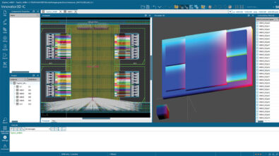
Innovator3D IC provides a consolidated cockpit for constructing a digital twin — featuring a unified data model for design planning, prototyping and predictive analysis — of the complete semiconductor package assembly. This cockpit drives implementation, multi-physics analysis, mechanical design, test, signoff, and release to manufacturing.
By unifying power, signal, thermal, and mechanical stress analysis tools, it enables rapid ‘what-if’ exploration, while identifying, avoiding and solving challenges prior to detailed design implementation. This shift-left approach can prevent costly and time-consuming downstream rework or suboptimal results.
Siemens already had the most comprehensive portfolio of semiconductor packaging related technologies available as part of Siemens Xcelerator, by combining these with Innovator3D IC we enable customers to achieve the realization of more-than-Moore.”
AJ Incorvaia, Sr. VP of Electronic Board Systems at Siemens Digital Industries Software
Innovator3D IC provides a unified cockpit
Innovator3D ICs unified cockpit is for design planning, prototyping and predictive multi-physics analysis. This cockpit constructs a power, performance, and area (PPA) and cost optimized digital twin of the complete semiconductor package assembly that in turn drives implementation, multi-physics analysis, mechanical design, test, signoff, and release to fabrication and manufacturing through a managed and secure design IP digital thread conduit
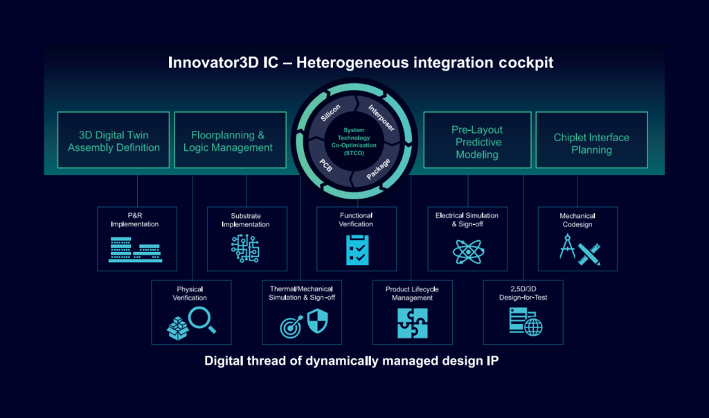
Innovator3D IC open architecture built around STCO
Innovator3D IC is architected around the system technology co-optimization (STCO) methodology process developed by IMEC. STCO is utilized throughout prototyping and planning, design, sign-off, and manufacturing hand-off, concluding with comprehensive verification and reliability assessment. Although the Innovator3D IC cockpit is directly integrated with the extensive Siemens Xcelerator technology portfolio, it supports the integration of third-party point solutions, recognizing that customers may have incumbent third party tools in their current design flows that they wish to continue using.
Single digital twin data model of entire assembly
Innovator3D IC constructs and maintains a 3D digital twin of the entire device including chiplets, interposers, substrates, and even the system PCB. Through its hierarchical device planning capability, chiplet and ASIC floorplans and their external interface assignments can be defined and optimized for overall PPA and cost targets. A hierarchical ECO flow with PANDR implementation tools allows for localized optimization of the individual chiplet, ASIC, interposer, package PPA and timing as well as with the overall device.
Industry standards support
A key tenant of Innovator3D IC is the support of industry standard formats, protocols, and API interfaces. The first key area is the commitment and support for the 3Dblox™ standard that enables EDA tool interoperability, bringing the benefits of improved productivity and efficiency to end users and customers in 3D IC system level designs. The next is to ensure frictionless adoption and consumption of existing and new die-to-die inter[1]face IP, such as UCIe and BoW. The Open Compute Projects Chiplet Design Exchange Working Group (OCP CDX) has enabled direct consumption of standardized chiplet models that will be provided by the emerging commercial chiplet ecosystem
Hierarchical device planning
Advanced 2.5/3D heterogeneously integrated designs containing multiple chiplets commonly have pin counts in the hundreds of millions. Designers face a major bottleneck in design assembly and ECO updates with such designs. Using only a top-level synthesis approach causes gaps for most practical applications, while taking analysis to the bump level everywhere is very time and resource consuming. Innovator3D IC uses a hierarchical device planning approach, which represents designs as geometrically partitioned (smart pin) regions with para[1]metric attributes. These attributes indicate how each region should be elaborated, using hierarchical reuse, and physically implemented, using known good layout techniques. Designers can thus quickly implement critical updates while matching analytic methods to specific smart pin regions to avoid extremely high execution times.
Chiplet to chiplet interface planning
Inter-chiplet communications are crucial to deliver the performance and bandwidth needed by high-performance computing and AI devices while meeting power requirements. Hierarchical interface route path sketch planning allows designers to explore interface route path channels and optimize chiplet interface and pin assignments. The results are passed to detailed place-and-route for PDK correct implementation.
Predictive multiphysics analysis
During prototyping and planning it is critical to evaluate the performance of all design scenarios before committing the design to implementation. Innovator3D IC integrates directly with power, signal, thermal, and mechanical stress analyses so that a design scenario can be evaluated quickly and any issues explored and resolved prior to detailed design implementation. This shift-left approach prevents costly and time-consuming downstream rework or sub-optimal results
Comprehensive workflow support
Once a system’s architecture has been partitioned or decomposed into its various implementation targets — such as chiplets, 3DSoC, ASICs, and memory — Innovator3D IC drives a set of comprehensive workflows, using a dynamically managed digital thread data model of the assembly’s digital twin.
For advanced heterogeneous integration platforms such as EMIB, an integrated floorplanning and prototyping cockpit with predictive analysis is essential – through our collaboration with Siemens EDA, we see Innovator3D IC as an important design technology component for our advanced integration platforms.”
Suk Lee, VP & GM of Ecosystem Technology Office, at Intel Foundry.
Built on next generation electronic systems design
Innovator3D IC is built on the same architecture as our next generation electronic systems design. This architecture delivers new capabilities in five key ways:
- Intuitive
- AI-infused
- Ecosystem connected
- Integrated
- Secure
Innovator3D IC drives ASIC, chiplet and Interposer implementation using Siemens’ Aprisa™ software digital IC place and route technology, Xpedition™ Package Designer software, Calibre® 3DThermal software, NX™ software for mechanical design, Tessent™ Test software, and Calibre® 3DSTACK software for interchiplet DRC, LVS and tapeout signoff.
Learn more about Inovator3D IC
Innovator3D IC is expected to be available later in 2024. To learn more about Siemens’ Innovator3D IC software Click here
Download the Innovator3D IC brochure: Click here
Read the press release Click here


Comments
Leave a Reply
You must be logged in to post a comment.
The next is to ensure frictionless adoption and consumption of existing and new die-to-die inter[1]face IP, such as UCIe and BoW. The Open Compute Projects Chiplet Design Exchange Working Group (OCP CDX) has enabled direct consumption of standardized chiplet models that will be provided by the emerging commercial chiplet ecosystem Solar