How to avoid delays in field-programmable gate array & application-specific integrated circuit projects

Most field-programmable gate arrays (FPGA), and often also application-specific integrated circuits (ASIC):, could be designed far more efficiently and with fewer bug iterations at all levels. By efficiency, one should consider detected delays and the fact that we could reduce a lot of wasted time already included in our planning. The same principle applies to bugs. There are always going to be bugs in complex designs, but there are far too many.
In fact, we have a huge improvement potential for both development time and quality. The best way to realize most of this potential is a good design architecture. Using on top of the Questa functional verification environment from Siemens EDA will further drive up the improvements.
Avoid delays and bugs
There could be many reasons for delays and/or the bugs mentioned above, but bad architecture is the most common. It doesn’t even have to be bad, but it’s just not good enough for the given specification complexity. As a design center for various customers, we often see this problem, strangely enough, in designs from both customers and their consultants. The root cause for this is that digital design architecture and making good block diagrams is not something students learn at the university – or at least very far from sufficient. What is quite a bit worse is that a significant number of experienced designers also do not handle this correctly.
Industry examples of bad architecrure
Through more than 20 years as a consultant, I have seen and heard of many extreme consequences of lousy architecture. These are just some examples of actual product delays:
- One year delay after “design is ready,” due to numerous iterations of patching and testing
- Eight months delay caused by not being able to achieve timing closure
- Eight months delay, due to not handling the required functionality
- Six months wait due to terrible state machines
All of these were only or close to only caused entirely by lousy architecture. I have seen similar examples of bugs escaping all tests and turning up in the customers’ products, which is mainly caused by a bad architecture. These examples might look extreme, but there are many similar examples – and of course, even more examples with “only” half the delays. The Wison Research Group study, commissioned by Siemens EDA, states that about 2/3 of the design projects are behind schedule. This trend has continued to be true since at least 2012. Logical/functional flaws responsible for bug escapes are dominating with about 50%.
Need a microarchitecture all the way down
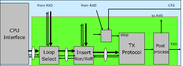
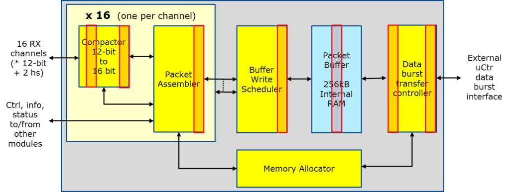
In most projects, there is a well-defined top-level architecture with clearly defined high-level modules, bus systems, reset and clock systems, etc. However, – very few projects have defined the microarchitecture all the way down. Many designers and project managers make lots of excuses for not doing this, but it is proven again and again that such a microarchitecture is by far the best approach.
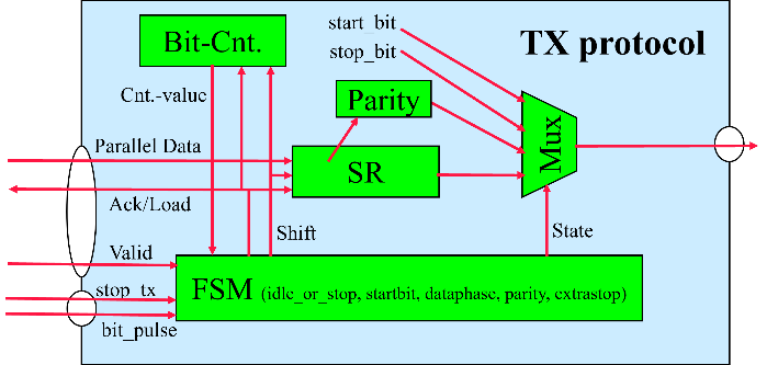
The initial figure and the figure above are typical examples of microarchitectures, clearly showing the architecture inside a module. In contrast, the figure below takes this one step further and shows the lowest microarchitecture level in a communication interface. While this is quite detailed, it reduces the total development time and improves the module quality.
Good architecture influences everything
I have concentrated here on how the design architecture affects development time and product quality, but in fact, a good design architecture will also improve other crucial aspects of field-programmable gate array (FPGA) and application-specific integrated circuit (ASIC) design:
- Power consumption
- Timing and Timing closure
- Verification space
- Simpler debugging
- Modified reuse
- Specification changes and Iterations
- Corner cases
- Walkthrough and Review
Strangely enough, there seems to be very little attention on these aspects in the universities and most Digital Design courses, which is why these aspects have been given extra attention in our two-day design course.
Verification architecture is equally important
The verification architecture does not affect the FPGA timing or Power consumption, but it certainly significantly affects the total development time and final product quality. For Very High-Speed Integrated Circuit Hardware Description Language (VHDL) verification, however, Universal Verification Methodology (UVVM) comes to the rescue. It provides a very structured testbench architecture, allowing the testbench development time to be drastically reduced while at the same time significantly improving the functional coverage. Siemens EDA is a key supporter of UVVM via the Questa Advanced Verification platform.
The architecture paradox
Making a good design architecture, unfortunately, has one bizarre side effect. Creating outstanding architecture for a rather complex specification, other designers – and reviewers in particular – will think ‘this was a simple task.’ Compared to a rubbish architecture where nobody has a chance to understand the code and design properly and are just impressed that you managed to get such a complex module to work at all.
The only sensible solution
A good Design Architecture will help you reduce development time, increase quality, and improve all-important design characteristics. Unfortunately, this is not fully understood or neglected by project managers and the designers themselves. Therefore, better awareness of the benefits of an exemplary architecture is perhaps a priority in most companies. As it really should be, but it is currently not priority one.
Then it would be best if you assured that your designers know or learn how to make a good design architecture. Introduce implementation proposal and early architecture walkthrough/review in your development flow, and of course, ensure that a good design architecture becomes a part of your development culture. If you would like guidance with your FPGA or ASIC design please visit EmLogic.
About EmLogic and the author
EmLogic is a leading Nordic design center for field-programmable gate array (FPGA) and Embedded Systems. As quality and efficiency are essential for our customers, architectural thinking is vital in our development methodology.
Espen Tallaksen, CEO of EmLogic, is the author and architect of UVVM and the founder of Bitvis (2012-2019) and EmLogic (founded January 2021). He has a strong interest in methodology cultivation, pragmatic efficiency, and quality improvement, and he has given many presentations at various international conferences with great feedback. He has also delivered courses on FPGA Design and Verification on three different continents.
EmLogic is a Siemens Digital Industries Software Software and Technology Partner. Software and Technology partners are leaders in their domain and leverage the open Xcelerator portfolio to provide customers with a comprehensive set of integrated solutions.


