FPGA and ASIC development rely on overview and readability

Quality and development time are critical parameters for Field Programmable Gate Array (FPGA) and Application Specific Integrated Circuit (ASIC) device developers, but there is significant potential for improvement in most projects. Thus, it is essential to evaluate how to exploit this improvement potential.
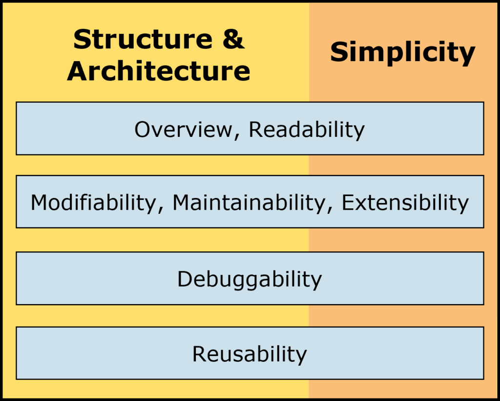
Overview and readability are critical for all improvement parameters
The figure above is a compact summary of the essential parameters for improving quality and efficiency. These are all crucial for suitable FPGA and ASIC development. Still, if you go deeper into each parameter, it is apparent that overview and readability are either vital parts or requirements of that parameter.
Readability refers mainly to how easy it is to understand the actual code and, of course, the interfaces of that code. Overview refers to how easy it is to understand the total picture, whether how two pieces of code interact at a low level or how the top-level modules work together. Thus, readability and overview are partly overlapping. So, high readability yields a better overview, and a better overview produces high readability.
Keep modifiability in mind during FPGA and ASIC development
Modifiability, maintainability and extensibility also overlap slightly. Modifiability and maintainability refer to how easy it is to understand and make safe changes to your design or test bench. The term modifiability applies to adapting and changing functionality during development. Maintainability describes changes due to bugs and later improvements. Modifiability is particularly useful when the specification is not stable or an architectural change is required, for instance, to allow a higher frequency or throughput. Extensibility refers to extending the functionality rather than just changing it and, thus, is often a more complex process.
Of all FPGA and ASIC development parameters, overview and readability are paramount. Any non-trivial change might be hazardous and time-consuming without a good overview and readability. However, it can be difficult to see all consequences of non-trivial code or block changes. It is not uncommon that fixing one problem leads to another somewhere else. The same applies when adding new functionality – even when the new functionality is quite simple.
By designing for these parameters, most companies could realize efficiency improvements of 20 to 50 percent on typical projects. There is potential for 200- to 300-percent efficiency improvements on troublesome projects and complex modules. Still, most companies do not seem to apply this sufficiently in their development process. This probably results from a lack of awareness and misunderstanding of the consequences.
Good design and debuggability go hand-in-hand
According to the 2020 Wilson Research Group Functional Verification Study, debugging constitutes around 25 percent of the total FPGA and ASIC development work, which is likely far more than most people are aware of and, therefore, not given the attention it deserves.
Two main aspects are important here. First, and most obvious, we need to improve debugging efficiency. This can be achieved by improving the structure and overview of test benches and the readability and controllability of test cases. Quality and readability of the transcript from the simulation, generated by a well-structured test bench and test case, are integral.
Second, and perhaps less obvious, is that a good FPGA design or ASIC design makes it easier to find the bug’s root cause – and even better – significantly reduces the number of bugs in the first place. Again, it is all a matter of overview and readability.
Reusability is ideal
The term reusability can be applied in many ways – for both design and verification. Plug and play reuse is the most efficient but is challenging to achieve since it depends 100 percent on direct reuse with no modifications. The opposite would be the “default” reuse, where you make a new variant based on a legacy design or test bench. The problem with default reuse is that it relies on unprepared modifications and is, thus, error-prone and time-consuming.
In most cases, the best approach is to design for modification and extension. By doing so, you significantly simplify and secure the reuse of previous designs and test benches. The most common argument against this approach is based on an assumption that it is too time-consuming. However, as previously discussed, this is, incorrect. Designing for modification and extensibility may take slightly more time upfront but reduces FPGA and ASIC development time significantly down the line, and also results in better quality. Again, overview and readability are vital to both efficiency and quality. So, the question is: “How can we achieve all the benefits mentioned?” The answer is quite simple and costs nothing.
The answer is in the architecture
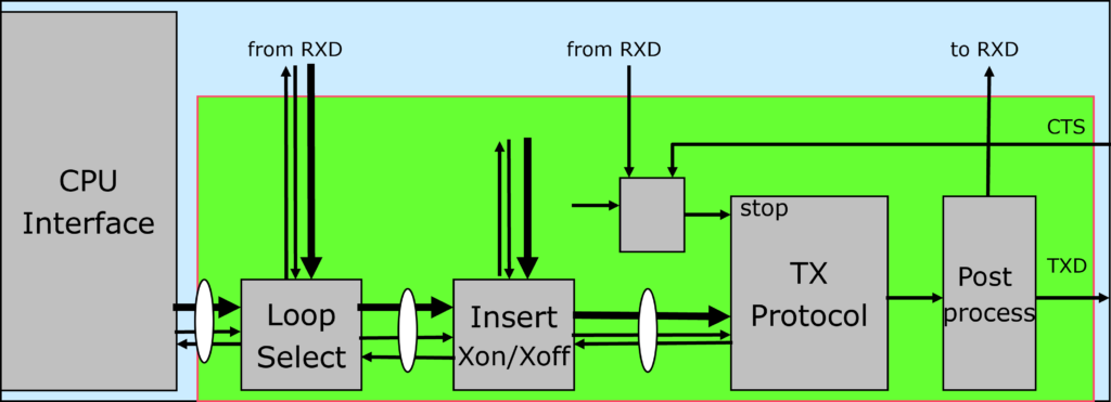
Architecture is always the most crucial aspect of developing a design or a test bench. Most know this, so the top level of any design usually has good architecture. Unfortunately, however, the same attention to architecture is not given to test benches. Also, there is often a severe lack of lower-level architecture called microarchitecture in both design and test bench development. While initially used for the lower-level architecture of a microprocessor, the term microarchitecture also applies to the lower-level architecture of any complex module. The microarchitecture for a universal asynchronous receiver-transmitter (UART) Tx module is shown, as an example, in Figure 2.
For any complex design or test bench, good microarchitecture is required to get a high-quality overview. The better the microarchitecture, the easier it is to read and understand the lower-level code.
Many developers consider “good architecture” synonymous with “well-structured design.” Whether this is accurate depends entirely on how you develop the architecture. Overview and readability, at all levels, should be the highest priority; otherwise, you will, in my opinion, not get good architecture.
Architecture is about layering your design or test bench and then “divide and conquer.” In software, one often also talks about “maximum cohesion and minimum coupling.” This has so many advantages – both for design and verification.
Examples of good architectures
Good design architecture is essential for quality and efficiency, power consumption, timing closure and many other critical design parameters. For some examples, read my blog from October 2021 on “How to avoid delays in field-programmable gate array & application-specific integrated circuit projects.” Test bench architecture is almost as important as design architecture for efficiency and, to a great extent, quality. In fact, for verification of a complex design, the test bench architecture can provide an excellent overview of the complete test bench, with all the individual verification components and the Lego-like connections between them. Figure 3 illustrates this. You can read more about this topic in my article “UVVM – VHDL Verification Methodology for Faster and Better FPGA and ASIC Verification.”
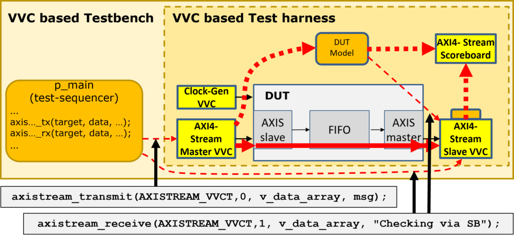
An important detail not illustrated in Figure 3 is that a single test sequencer can control all of the DUT (device under test) interfaces. This unique feature of the methodology produces the best possible overview and readability.
Efficiency and Quality in FPGA and ASIC development
Overview and readability, good architecture, simplicity and all the other elements of a successful project illustrated in Figure 1 are not overly challenging to produce. However, getting all project managers and associated functions to accept their significance may present a challenge. For example, allowing enough preparation time before starting to code could create conflicts with the traditional project schedule.
Prioritizing overview and readability will likely require most companies to re-evaluate their entire development approach, which may be a painful process. However, the alternative will be much worse.
Learn more about creating a test bench using the Universal VHDL Verification Methodology (UVVM) in Xcelerator Academy.
About the author
Espen Tallaksen, CEO of EmLogic, is the author and architect of UVVM and the founder of Bitvis (2012-2019) and EmLogic (founded January 2021). He has a strong interest in methodology cultivation, pragmatic efficiency, and quality improvement and has given many presentations at conferences globally with great feedback. He also offers courses on FPGA Design and Verification worldwide.
About EmLogic
EmLogic is a Software and Technology Partner and leading Nordic design center for field-programmable gate array (FPGA) and Embedded Systems. Architectural thinking is vital to EmLogic’s development methodology because quality and efficiency are essential to customers. For more information about EmLogic, UVVM, and our courses visit its website.
Partners who build solutions
Software and Technology Partners use the Siemens Xcelerator portfolio and its flexible open ecosystem to build technologies that complement the comprehensive digital twin and provide customized solutions for our mutual customers. These partners often develop, sell, support, and market hardware and software solutions that are interoperable with Siemens products and ensure infrastructure compatibility. Find a partner to help you build your digitalization solution.


