The new VX.2.13 release of PADS Professional has improvements for the following features in PADS Professional layout. Enhancements to the…
The new VX.2.13 release of Xpedition has improvements across three key areas: Layout, data management, and verification. Improvements in Layout…
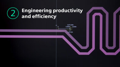
When we think about the PCB design best practices that fall into the engineering productivity and efficiency pillar, we need…
With increasingly advancing technology and faster edge rates in today’s integrated circuits, it’s important to find more efficient ways to…
We can’t believe its already been a few weeks since returning from IPC APEX 2023. Siemens and Boardera started collaborating…
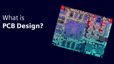
What is PCB design? PCB design is the entire process of creating a Printed Circuit Board (PCB) through collaboration and…
As I outlined in my first blog, there are five pillars of PCB design best practices. The first pillar we…
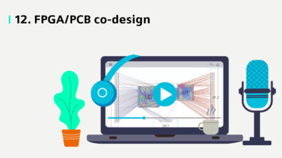
As the complexity of today’s designs continue to increase, more electronic product designers are turning to Field Programmable Gate Arrays…
Previously… People often say ‘better late than never’, but I’ve never heard my boss say that. After much difficulty in…