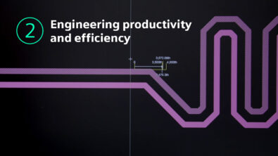
PCB design best practices pillar 2: engineering productivity and efficiency
As I outlined in my first blog, there are five pillars of PCB design best practices. The first pillar we discussed was “digitally integrated and optimized.” The second pillar I’m going to focus on is “engineering productivity and efficiency.”
Today I will talk about how to optimize engineering productivity and efficiency to reduce design cycle time, reduce costs, and lower risks.
In general, PCB design is the same no matter which company you work for, what team you’re on, or what culture you belong to, but the differentiator is execution. And it plays a significant role. Engineering productivity and efficiency enables you to predictively and reliably manage complex, high-capacity designs. It allows you to utilize advanced, interactive automated design support to accelerate routine tasks. It also assists in design correct by construction with constraint driven processes. And it assists in implementing concurrent team design driven design cycle time reduction.
Within this second pillar there are several PCB design best practices to highlight:
Design automation
Assign parts to groups or clusters by utilizing a combination of interactive and automated routing strategies. You can also generate manufacturing outputs by utilizing built in automation functionality. Using design automation results in shortened design cycle times and increased layout efficiency. In the end, you’re going to get the ability to do “what if” scenarios, review and implement changes more efficiently, while removing potential errors. And lastly, you’ll be able to have consistent manufacturing outputs.
Concurrent design
Use advanced capabilities for collaboration while in schematic and layout phases on design. With concurrent design in the schematic, you can have two or three users working at once. You can also have several Electrical Engineers (EEs) working in the schematic at the same time. You could also have multiple PCB designers working in the layout at the same time. Have multiple EEs in the front end, which is the schematic, as well as having multiple designers in the back end working in the layout. Everyone can be working simultaneously in one project/design at the same time. Think about how many hours you can save by attacking your design with multiple users at the same time. It allows you to optimize multidiscipline integration in the design database as well as optimized project team utilization. In the end, designs potentially can completed with better quality by construction, more efficiency and streamlined in the overall process, and lower overall project costs.
Design reuse
As a best practice, you want to utilize existing known good circuitry and proven layouts that have been tested and validated, so you’re not reinventing the wheel with each design. You want to be able to manage the reuse modules no differently than you would manage a single component in your library. And then you want to be able to share that hardware IP, not just from design to design within your business unit or within your local area, but if you have a huge enterprise that’s global, you want to be able to share that IP globally. That way, you can take advantage of designing whole systems a lot faster with more potential for success on the first revision. This best practice will reduce your design cycle time, which will also reduce costs, and lower risk.
Constraint-driven design
Create an automated way to manage design constraints, so that you have them to use design after design. It allows you to control your electrical and/or physical rules and HW requirements. This way, you’re going to design quality into your board and not simply going to check for quality only after the fact and hoping you get it right. With these rules in place by utilizing a constraint-driven design approach, you’re going to have confidence that you’re meeting your requirements because you eliminate the human factor of having to go back and manually check and validate your design. Constraint-driven design is the process of checking as you’re designing the board, in real time.
Advanced design
Using the opportunity for rigid flex methodology within our tool sets allows a more efficient way to define a board outline as well as the required PCB stack ups and regional constraints that may be required to have. When you think about a rigid design or rigid flex, you’d have a rigid section, you have a flex section, and then another rigid section. These different sections combined make up the entire design. This leads to having multiple stack ups in one design. One stackup in the rigid area, and then another, yet different stackup in the flex area. It can cause a lot of confusion, especially if you’ve never designed a rigid-flex design it before. But our tools are more than capable of doing this in one design database versus having the need for multiple databases. This affords you a more efficient way to design complex systems and provides a way of optimizing signal flow from board to board. This rigid-flex design approach helps eliminate connectors.
When you talk about high pin count BGAs and other high pin count components, especially as the pin pitch gets tighter and tighter, sometimes you must implement High Density Interconnect (HDI) approach simply because you chose a part with a tight pin pitch, requiring the need to implement HDI to design a specific component in. Designing with HDI does provide an advantage, when implement, by eliminating workarounds, as well as the ability to add complexity to designs. There is a cost factor that must be considered, regarding HDI, but early collaboration with your PCB fabricator helps to mitigate risks while meeting your design intent/requirements, and potentially reduce costs.
Engineering productivity and efficiency
In conclusion, by utilizing today’s tool’s horsepower and capabilities regarding engineering productivity and efficiency, we can significantly optimize the design approach to be more efficient, better optimized, and produce higher quality designs, while having the best potential to lower project risks.
As we continue along in this series I will zero in on each best practice within this pillar and provide examples of how to implement them, address challenges and overcome roadblocks.
Thanks for following along and make sure to check out the full video on engineering productivity and efficiency here.