PCB design best practices: thermal analysis
Designing today’s complex PCB is no easy task. It requires a full understanding of the basics of PCB design, a mastery of your CAD tools, the ability to effectively work in a team environment, and a thorough understanding the entire design process flow. Add in manufacturing (both fabrication and assembly) complexities, vague or incomplete customer requirements, shorter project schedules, limited resources, and reduced project budgets and it can be brutal at times. Knowing and implementing the industry’s PCB design best practices is the key!
Today I want to talk about best practices when it comes to thermal analysis as a part of pillar 3: digital prototype-driven verification.
What is thermal analysis?
Thermal analysis will check/verify that all hot spots within the design are mitigated and optimized to ensure the best potential for your PCB to perform as intended prior to fabrication.
What’s not working today?
Today’s complex PCB designs are more challenging than ever before due to fast signal speeds. We are seeing more and more PCB designs with signal speeds in the gigahertz, especially in high-speed designs where we are dealing with edge rates of signal switching speeds that are the fastest they have ever been. As if that wasn’t enough to deal with, we now have physical component packages that have shrunk smaller than ever and continue to do so, and we are seeing more and more use of exotic PCB materials in attempts to mitigate heat issues with regards to the thermal performance of the PCB/PCBA.
Thermal management in PCB design is serious business, to say the least. High-power telecommunication and mil-aero applications were the main sectors in the industry where we would typically see these types of complex challenges. Now, we see such complexities in designs that have made their way into the automotive, consumer electronics, and medical sectors of our industry. It’s has become the new normal.
In general, a PCB typically starts in the mechanical world. It is the mechanical engineer who starts the creation the physical envelope in which this PCBA will reside from the customer requirements. In this world, addressing the thermal characteristics that will enhance the mitigation of removing heat from the widget being created, not just from the box, but from the PCB/PCBA as well. PCB material, airflow, and heat sinking all come into play. In challenging complex PCB designs, this is serious business! Not getting this right can potentially be catastrophic! From copper traces popping life fuses, to components overheating, to PCBAs catching on fire. There is no room for simply guessing and hoping your design will work as intended when your product gets into the market.
What are the roadblocks?
Typical roadblocks that stand in the way of implementing thermal analysis have more to do with project pressure. Basically, a last-minute decision by project management to reduce the project budget and to pull in the project schedule. Many times, a project is running behind schedule and there are budget over runs, which tend to push individuals to make a last minute decision to accept the risk in releasing a design prematurely, by foregoing required analysis such as a SI, PI and or thermal analysis, even though it was planned in the project schedule.
Another typical roadblock is the lack of a specialist or having access to engineering tools within the industry such as Simcenter FLOEFD and Hyperlynx. These are a good example of tools that improve electronics thermal management for reliability with fast, accurate electronics cooling CFD simulation from initial pre-CAD exploration to final verification. Of course, a related roadblock is access to models, once you’ve made the decision to simulate.
Best practices: thermal analysis
There are 3 main best practices when it comes to thermal analysis.
1. Close collaboration and integration in this multi-domain environment between mechanical and electrical engineering disciplines is a must! This includes ECAD and MCAD domains as well. Close collaboration with fabrication/manufacturing is the final piece of this thermal management solution puzzle.
Once the mechanical attributes are dialed and locked in, the physical envelope to which the PCBA will reside, is now set and handed off to ECAD. This is where the initial bi-directional collaboration between MCAD and ECAD begins. The best practice is to have an automated seamless integration between these two disciplines and their respective tools.
There are several methodologies for data exchange, but the IDX format for data exchange is today’s best practice. In this format, the physical intelligence of the rules being passed back and forth include features such as board outline, board thickness, keep out/in zones, component height/ceiling restrictions, tooling holes, mounting holes, slots, heat sink locations, and any critical component location requirements, etc.
2. Component placement is critical. A good component placement addresses both the physical and the electrical requirements of the design. From addressing the need for pulling heat away from critical components to having an optimized routing flow and strategically utilizing thermal vias in the design is key to success! Even with implementing best practices up to this point is not enough with regards to today’s complex PCBAs. This is where the performance analysis of the PCB comes into play.
3. It’s vital that a thorough analysis is done at components placement and then again when the PCB is completed. There are several tools in the industry that are specifically designed to do this analysis. Some better than others, especially with regards to multi-tool integration/collaboration and functionality.
A good thermal analysis will check/verify that all hot spots within the design are mitigated and optimized to ensure the best potential for your PCB to perform as intended and for downstream success of your product when it gets into the field and or released to market. If, and when thermal issues are addressed early in the process, adjustments are easier to accept, versus dealing with them late in the process. It’s vital that this thermal analysis be done! This is not a step in the design process that should be skipped simply to save a few bucks in the project budget, and or time in the project schedule. Make no mistake, not completing a thorough thermal analysis will come back to haunt you. So it’s very important that your design be created correct by construction to address the proper performance regarding the thermal management solution for your design.
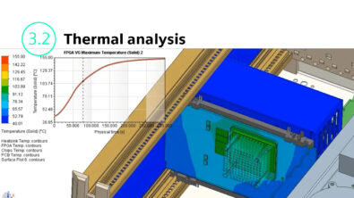
How it works: thermal analysis
Exploring the thermal characteristics of a design can be done as soon as board 3D geometry is created, not necessarily when the design is complete. Thermally relevant information, such as fan velocity if the system has fans, and heat sinks, are considered. Running the simulation of a board within the chassis of the product makes sure that users get the most realistic results from the simulations run.
Several different types of data can be extracted from analyzing the digital prototype. For instance, temperature distribution of the electrical and mechanical components, air velocity within the design, and even data about the temperature change over time can be captured, making it easy to optimize the thermal performance of the end product.
To learn more about thermal analysis watch this video: