Enhancing EUV lithography resolution at high numerical aperture
By Ethan Maguire
As the semiconductor industry continues to push the boundaries of feature size and density, the need for novel lithography techniques has only increased. One area that has garnered significant attention is the use of extreme ultraviolet (EUV) lithography for high numerical aperture (high-NA) applications.
In a recent paper presented at SPIE Advanced Lithography 2025 by researchers from Siemens Digital Industries Software, we explore a novel approach to enhancing resolution and depth of focus for EUV lithography under high-NA conditions. The key to our solution lies in the use of aperiodic multilayer masks, which offer significant advantages over conventional periodic multilayer designs.
The multilayer mask problem and an aperiodic solution
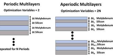
Conventional periodic multilayer masks used in EUV lithography are structured as repeated layers of silicon and molybdenum with a patterned absorber on top. This periodic design worked great during the 0.33 NA era and can perform well under 0.55 high-NA conditions too. However, the 3D nature of these masks leads to optical interactions, like shadowing, X-Y image variation and through-focus image shifting. These effects can degrade imaging metrics such as normalized image log slope (NILS), a critical indicator of pattern fidelity. As the numerical aperture of EUV systems increases to enable higher resolution, these 3D mask effects become even more pronounced.
We propose the use of aperiodic multilayer masks to address the limitations of periodic masks. In an aperiodic mask, each layer has a unique thickness, allowing the mask to be optimized for improved reflected intensity, phase, polarization and spectral bandwidth. Figure 1 shows the structural differences between periodic and aperiodic multilayer masks.
Aperiodic multilayer masks provide a new optimization paradigm for EUV lithography. By moving beyond the constraints of periodic designs, mask engineers can jointly optimize NILS, depth of focus and other critical metrics to deliver superior imaging performance.
The integration of aperiodic multilayer masks into the EUV lithography workflow will be a crucial next step. The Calibre pxSMO tool (Source Mask Optimization), which was used in this research, provides a comprehensive platform for mask optimization and simulation that can be easily incorporated into existing flows.
Validating aperiodic multilayer designs with the Calibre pxSMO tool
To validate the performance of the aperiodic multilayer design, we used the Calibre pxSMO tool, a resolution enhancement software that allows for detailed analysis and optimization of the lithography process, including the mask design.
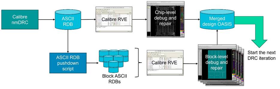
The Calibre pxSMO simulations confirmed the significant improvements in NILS and depth of focus provided by the aperiodic multilayer, compared to a conventional periodic design. For both vertical and horizontal mixed-pitch line/space patterns, the aperiodic multilayer demonstrated NILS gains of up to 26% and over 130 nm improvement in combined depth of focus. Figure 2 shows the results for vertical patterns (left) and horizontal patterns (right) of mixed pitch [18, 24 nm]. The top image shows the aperiodic mask and the lower image shows the conventional periodic mask.
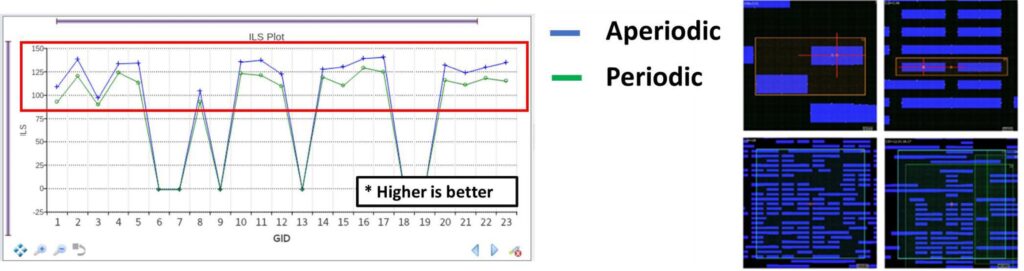
Additionally, for a more complex metal layer test case with a fixed illumination source, the aperiodic multilayer showed higher image log slope (ILS) across all measured features, indicating better overall printing performance. Figure 3 shows image log slope data measured by Calibre pxSMO for the metal layer type layout.
Conclusion
As the semiconductor industry continues to demand ever-smaller feature sizes and higher device densities, the need for innovative lithography solutions has never been more pressing. Our research on aperiodic multilayer masks for high-NA EUV lithography represents a significant step forward in addressing these challenges.
By optimizing the mask design to enhance critical imaging metrics like NILS and depth of focus, we demonstrate a path forward for reliable, high-quality patterning at the leading edge of semiconductor technology. As the industry adopts this new optimization paradigm, we can expect to see continued advancements in EUV lithography and the realization of the next generation of integrated circuits.


