Solving IR drop and layout bottlenecks: How Calibre DesignEnhancer streamlines IC design
By Jeff Wilson
As an IC designer, you know that achieving an optimal layout is about more than just meeting design rule checks—it’s about balancing electrical performance, manufacturability and time-to-market pressures. A well-optimized design not only reduces costly iteration cycles but also ensures better performance and faster time-to-market. Yet, despite advanced design tools, meeting stringent DRC while optimizing for electromigration and IR drop (EMIR) remains a significant challenge.
IC designers require tools that streamline design flows while maintaining both yield and power integrity. As semiconductor layouts grow more complex, ensuring both DRC compliance and electrical performance can be challenging. Calibre DesignEnhancer (DE) offers automation-driven solutions to address these difficulties, helping designers optimize layouts efficiently. Let’s explore the key challenges IC designers face and how intelligent automation can enhance the design process.
The IC design bottlenecks: Challenges that slow you down
Place-and-route (P&R) tools do a nice job of inserting cells and connecting them. But because the P&R solutions don’t understand all the design rules, ensuring a DRC-clean design requires taking an overly conservative approach, which can limit the layout enhancing changes that can improve the EMIR results. As technology nodes shrink, maintaining a robust power delivery network becomes increasingly difficult due to higher transistor density and dynamic voltage drops. To deal with this complexity, automation is key in making physical design modifications to reduce design cycles. To a designer key automation steps include the reading of both the electrical analysis and layout data, making the layout modifications and then back annotating the results. Automated solutions need to understand all signoff design rules and honor them during the physical design stage. This shift-left approach ensures that the most accurate design rule descriptions are used for DRC checking, but you also have the flexibility in the layout to make the most effective modifications.
Calibre DE offers a different approach—one that combines DRC knowledge with automation to deliver both compliance and performance enhancements.
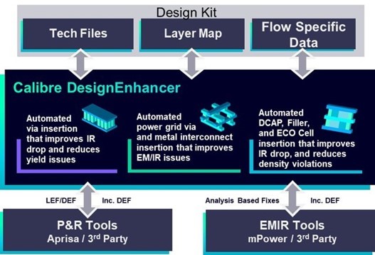
How Calibre DE optimizes IC design
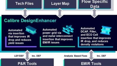
Calibre DE integrates seamlessly into existing design flows and provides targeted enhancements through three key use models that address time-to-market and power integrity. Calibre DE is designed to give users multiple layout enhancing solutions that that can be used throughout their design process. Currently Calibre DE has three use models in production.
1. DE Pvr: Fast-tracking time-to-market with automated physical verification readiness
When designing an advanced IC on the latest technology node, adding decoupling capacitors (DCAPs) and filler cells is an essential but very time consuming task. If skipped, physical verification (PV) runs will light up with DRC violations, but if done with the traditional P&R solutions, runtime can stretch into multiple hours. Calibre DE Pvr automates this process using the Calibre processing engine to quickly fill in the open spaces, thus reducing verification runtime from over 10 hours down to a few hours. This reduction in cycle time accelerates the path to production and minimizes last-minute surprises.
2. DE Pge: Addressing EMIR issues
As process nodes shrink, IR drop and electromigration (EM) become critical design concerns. Calibre DE Pge (Power Grid Enhancement) automate enhancement to the power delivery network (PDN) by:
- Optimizing power grid structures with DRC clean layout modifications.
- Inserting parallel paths with the required via insertion to reduce resistance and minimize EMIR issues.
These enhancements result in a more robust design that meets reliability requirements without increasing design size.
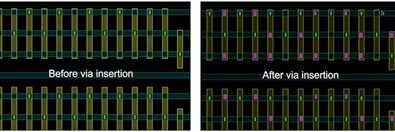
3. DesignEnhancer Via: Reducing the IR drop and improving yield
To address the manufacturing concerns caused by vias and to reduce IR drop, use Calibre DE Via (Via insertion) to optimize user defined netsby maximizing the number of DRC clean vias to reduce the resistance.
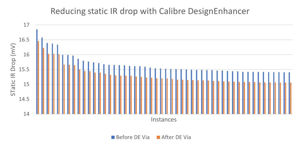
Case study: Google’s IR drop success at 3 nm
Google faced significant IR drop issues when transitioning to a 3 nm process node. While scaling to smaller nodes improved area and performance, it also introduced new power integrity challenges. Increased voltage drops arose due to higher transistor density, leading to more static IR drop issues caused by narrower and longer interconnects. Additionally, power delivery inefficiencies created performance degradation risks.
To address these challenges, Google leveraged Calibre DE’s automated via insertion and power grid enhancement. This approach resulted in a 30% decrease in the number of high-IR drop instances. The modifications remained DRC-clean, eliminating the need for additional manual iterations. Ultimately, Google improved power integrity without overdesigning the PDN, ensuring a more efficient and reliable design process. Read the whole case study here
Case Study: Intel enhances reliability with Calibre DE Via
Intel’s graphics team also turned to Calibre DE Via to reinforce their power grid. Initially, their P&R tool failed to insert the maximum number of vias, leading to weak power connections. The complexity of via rules at 5 nm—spanning spacing, width-based checks and via count requirements—made manual fixes impractical.
By leveraging Calibre DE’s detailed rule knowledge, Intel:
- Inserted 9 million additional vias on key nets.
- Improved power grid robustness without introducing new DRC errors.
- Achieved better electrical performance and yield. The chart below shows the via counts per net.
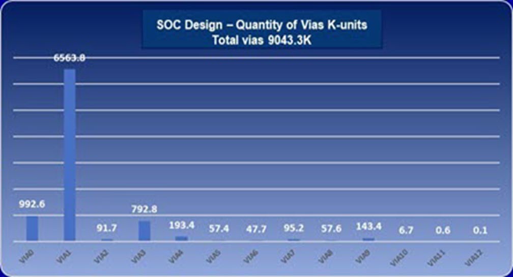
These results demonstrate how Calibre DE’s correct-by-construction methodology outperforms traditional P&R approaches. Watch the full story here.
The competitive advantage of correct-by-construction enhancements
Unlike conventional P&R tools, Calibre DE understands DRC rules at a deep level, enabling it to make aggressive yet compliant layout modifications. This capability leads to fewer design iterations and faster tape-outs, as well as improved electrical performance through optimized via structures and power grids. Calibre DE design kits offer solutions that span multiple foundries, supports multiple technology nodes and works with the leading P&R tools , to deliver the flexible IC designers need.
The bottom line? Calibre DE is a layout enhancement solution that ensures DRC compliance while maximizing design improvements with specific use models.
Seamless integration into existing design flows
Calibre DE integrates with industry-standard design tools, allowing:
- Industry standards such as LEF/DEF, OASIS and GDS formats to get data into and out of the various DesignEnhancer use models.
- Design kits make it very easy to deliver multi-foundry and IDM support, ensuring consistency across different fabrication processes.
By providing a flexible, automated approach to design enhancements, Calibre DE reduces complexity while improving design outcomes.
Conclusion: Smarter IC Design Starts with Calibre DE
As semiconductor design continues to evolve, the need for automated, rule-aware design optimization becomes more pressing. Calibre DesignEnhancer meets this need by providing correct-by-construction solutions that enhance power integrity, reduce design iterations, and accelerate time-to-market. Our recent technical paper that dives even deeper into this topic is now available: Google and Intel find success with Calibre DesignEnhancer
Whether you’re tackling IR drop, optimizing vias, or streamlining physical verification, Calibre DE provides the precision and automation necessary to navigate today’s IC design challenges.