Why PID issues matter to IC chip designers, and how to combat them
By Derong Yan
Integrated circuit (IC) chip designers are constantly striving to meet ever-increasing standards of reliability and performance in the fast-paced realm of semiconductor manufacturing. Amidst these challenges, plasma induced damage (PID) in gate oxide, often referred to as the antenna effect, stands as a significant threat to the yield and reliability of MOSFET circuits. While PID actually occurs during IC manufacturing, it can be minimized or eliminated by finding and fixing susceptible layout patterns during the layout design stage.
Traditional antenna design rules
Traditional antenna design rules check layer-by-layer for the maximum allowed area ratio between a metal (or via) layer and the MOSFET gate layer connected to the same net, as shown in figure 1(a). The addition of a diode protection device expands this maximum allowed area ratio, as shown in figure 1(b). Traditional design rule checking (DRC) flows easily and efficiently handles these checks.
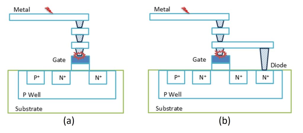
Figure 1. Traditional antenna DRC checks for area ratio between metal (or via) layer and MOSFET gate layer (a) without protection diode, and (b) with protection diode.
Evolving antenna challenges in IC chip design
In recent years, analog mixed-signal (AMS) designs have gained popularity due to their compact integration and reduced power consumption. AMS designs involve multiple power domains that create cross-domain design challenges. These challenges include the existence of isolated P-type wells, which has introduced a new generation of antenna issues that can’t be effectively addressed using traditional DRC checks:
- Risk connections: Identifying when a risk connection between driver and receiver is established before corresponding protection connection between two isolated P-type wells is established.
- Charging damage: Detecting imbalanced area ratios between metal (or via) layers and well layers from two isolated P-type wells.
- Connectivity waivers: Analyzing complex connectivity conditions that can waive antenna violations caused by imbalanced area ratios.
- Unintended protection diodes: Checking for unintended protection diodes formed due to connectivity, which increases the maximum allowed area ratios.
Path-based antenna verification and its significance in IC chip design
Addressing these complex antenna design rules requires an all-around solution that understands devices, connectivity, and electrical paths within IC designs while calculating metal and MOSFET gate layer areas. The good news? The Siemens EDA Calibre® PERC™ reliability verification platform enables designers to identify paths of interest in IC chip designs and perform intricate antenna rule checks on those paths, offering flexibility and efficiency.
Although this path-based verification approach is essential for addressing complex and evolving antenna design rules, traditional DRC-based antenna checking remains a valuable part of the verification process. The two verification flows complement each other, providing complete coverage of both traditional and advanced antenna design rules: During the early design stages, when connections are incomplete, traditional DRC checks can be used for preliminary antenna-related correct-by-construction checking. This verification ensures that layouts are constructed with PID prevention in mind, reducing the need for time-consuming fixes in later iterations. As paths form across isolated P-type wells, the path-based solution becomes indispensable to check more complex antenna design rules.
If you are an IC chip designer who is suffering from yield loss due to PID issues, the Calibre PERC path-based PID solution may be useful to you. Check out our technical paper for more details: Path-based antenna checks reduce PID susceptibility in IC designs (siemens.com).