Calibre IC manufacturing research for what comes next
By Germain Fenger
Director of Product Management RET modeling, Calibre Semiconductor Manufacturing Solutions
There is no rest in semiconductor manufacturing. By the time one process, or piece of a process, or materials, or method, is fully understood, the next big change is on the horizon and coming at us quickly. For Siemens’ Calibre group, staying ahead of the curve means engaging in research with industry partners.
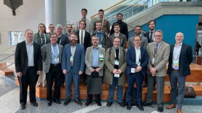
Siemens works with leading research hub, imec, who plays a crucial role in helping the semiconductor industry develop the latest technology and train engineers. Since 2013, imec has hosted permanent on-site engineers from Calibre. This type of deep collaboration pays dividends for Siemens EDA users.
Past and ongoing research
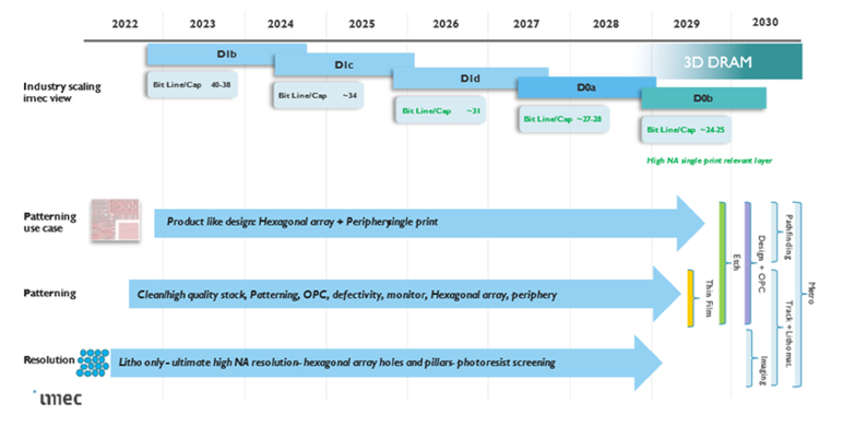
Research with industry partners that made it into Calibre tools in includes inverse lithography starting with DUV lithography (Calibre pxOPC), multi-patterning design decomposition for DUV and EUV (Calibre DP/MP), process modeling utilizing contours (Calibre nmModelflow and Calibre SEMSuite), OPC for EUV lithography (Calibre nmOPC), and fab analytics (Calibre Fab Insights).
Not all research projects lead directly to products. There are always competing technologies, with winners and losers, all of which must be explored. For example, directed self-assembly (DSA). This complementary lithography technology was one contender for improving resolution at the N7 process node. The industry ultimately went in a different direction, but DSA might be useful in the future. If so, Calibre is ready.
Current research
So, what are some of the current research projects that users will one day use in Calibre products? Top of the list is high-NA lithography. The NA (numerical aperture) controls the amount of light (or number of diffraction orders) that’s used to form an image. For extreme ultraviolet (EUV) this means moving from 0.33 to 0.55NA. The industry is moving quickly to adopt high-NA EUV, with equipment and tools ready for market. Our researchers have been engaged with this project since at least 2017. The results of that research will be available in Calibre computational lithography tools, including Calibre pxSMO, Calibre pxOPC, Calibre nmOPC, Calibre OPCverify, and Calibre nmModelflow. After high-NA is, of course, hyper-NA with .75NA. That technology is in the exploratory stages now.
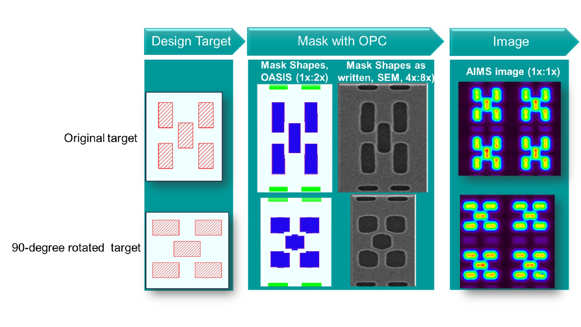
Another exciting project involves anticipated new mask materials. LAM, ASML and imec are developing a completely new photoresist material. This material promises better resolution, less line edge roughness (LER), and high light sensitivity. Traditionally, resist material is spun on to the wafer as a coating, then developed in an aqueous solution. These chemically amplified resists (CARS) have limitations starting at 5 nm node, mostly from image blur due to acid diffusion. The basic resist chemistry hasn’t changed in 50 years.
This new resist is close to being used for production. It is a dry resist; rather than spin-on liquid, it is applied using reactive precursors in a vapor phase in a vacuum system. The film is unform and homogeneous, and the high density is more efficient at capturing photons on the metal-oxide resist. It comes with plenty of new challenges for us due to additional physics like very long-range loading effects that we need to account for in our OPC models.
Other research
We also work with other companies, including JSR Corporation, on new photoresist materials. We engage with metrology companies, including Hitachi and AMAT, to calibrate compact OPC models and study how metrology impacts OPC models. We built tools that extract contours for OPC modeling with NGR Inc. and Hitachi, a technology that is now in high demand.
To round out the list, we have projects with imec on curvilinear data processing, field stitching for high-NA reticles, expanding advanced ILT solutions into the curvilinear domain, and identifying the root causes of hotspots and failures in complex processing sequences (which will be leveraged in a new set of fab tools in the Calibre product family).
Learn more about the Calibre IC manufacturing solutions.
Leveraging the collaboration, imec and Siemens EDA also participated in broader research efforts sponsored by the European Union, TAPES3, a project to prepare the technology infrastructure for the 3 nm semiconductor node, and MADEin4 driving manufacturing technology under the industry 4.0 paradigm. Our close partnership with imec gives us insight into what technologies might be needed in the future. If you don’t explore all these research projects, then our Calibre tools can’t offer the solutions our customers need. We are looking forward to the next twenty years of fruitful research and collaboration!