Electromigration protection requires accurate interconnect modeling
By Karen Chow, Mentor Graphics
Electromigration can destroy an IC before its time. Are your designs safe?

What is Electromigration?
Electromigration (EM) refers to the undesired migration of metal atoms along a metal interconnect. This migration occurs due to the “electron wind” (which is the momentum transfer created by electrons in the current) pushing the metal atoms that make up the interconnect. If enough of these atoms move, EM eventually causes voids and/or hillocks in the chip (Figure 1).
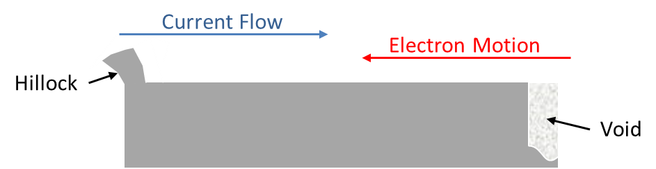
Figure 1. EM occurs when atoms are pushed from their position in the interconnect by the momentum of the current moving through that interconnect.
These hillocks and voids cause shorts or opens in the design, which lead to circuit malfunctions or total chip failure (Figure 2).
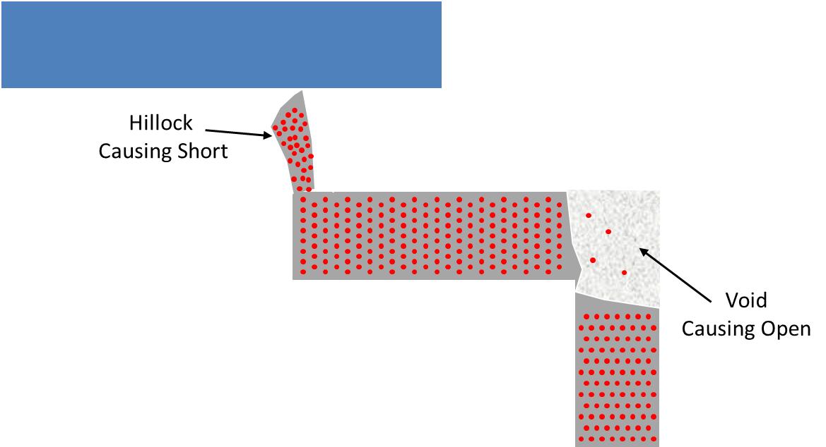
Figure 2. As EM causes metal atoms to migrate, hillocks can create shorts, and voids can lead to opens.
While EM damage is readily apparent in microscopic evaluations in the lab, it can be difficult to distinguish from other failures in everyday usage conditions, since initial symptoms are typically intermittent failures or seemingly random errors. Additionally, the EM effect happens slowly over time, although the acceptable mean time to failure (MTTF) depends heavily on the type of application. For example, cell phones are typically replaced every two years, so their MTTF can be relatively short, while space probes often have a projected product life of ten years or more, requiring an extended MTTF. The use model also affects MTTF—failure in a car radio is a consumer annoyance, while failure in an implanted pacemaker or other medical device can lead to death.
Determining the market’s tolerance for reliability failures is essential to determining how much EM protection to build into a given design. However, the protection process is identical for all levels of MTTF.
Mean Time to Failure and Black’s Equation
The projected MTTF due to EM is defined by Black’s equation:
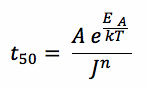
Where A = constant, J = current density, n = 1-3, EA = activation energy
A key part of measuring EM is to measure the current density (J). The higher the current density, the shorter the MTTF will be.
Designs can be modified to increase MTTF by reducing current density. There are two ways to reduce current density:
- Reduce the current flowing through a specific point in the layout by providing additional current paths
- Increase the width of the wire to spread (lower) the current density passing through that wire
Figure 3 illustrates these two techniques. The red square identifies a point where too much current is flowing though the via, raising the likelihood of EM failure. Adding a second via disperses the current between two vias, which reduces the current density at any one location, reducing the EM violation level. The designer could also widen the interconnect (wire spreading) leading to the via(s), giving the current more space to flow. This lowers the current density, again reducing EM. However, both of these techniques can cause design area to increase, so it is important for designers to understand and evaluate the trade-off between design area and long-term reliability.
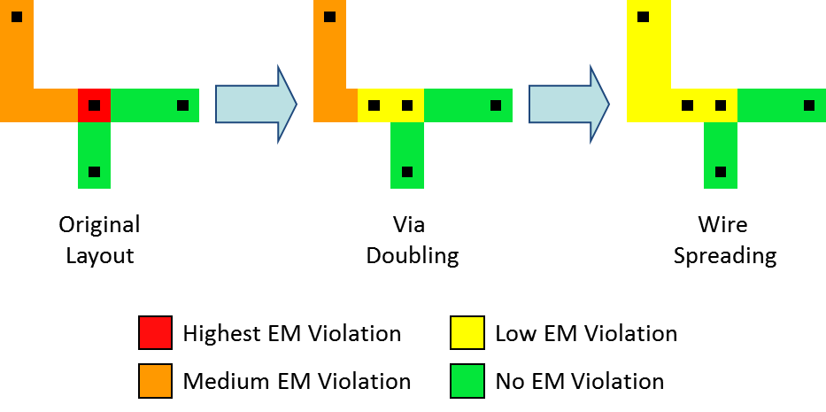
Figure 3. Via doubling and wire spreading are the two main design solutions for reducing or eliminating EM effects.
EM Challenges at Advanced Nodes
Although IC design reliability has always been an important consideration, the challenge of implementing EM protection has been increasing over the last few years, due to design shrink and lithographic limitations. At 16 nm and below, it has become particularly difficult, because the wires are so much thinner, causing both current densities and the parasitic resistance of these wires to increase. At older nodes, the focus for EM was directed at the power grid, but for 16 nm and below, long and thin signal lines combined with increased switching speeds increases the need to perform both dynamic and static EM analysis on these lines. The increased heating in high-frequency signal lines (caused by the interaction of electrons with the lattice of the interconnect) can produce thermal energy that further causes EM failures, so foundries are now adding rules for delta temperatures (temperature increases due to current) at advanced nodes. The introduction of finFET transistors also contributes to an increase in the drive current, which makes meeting the MTTF requirements even more challenging. Finally, as copper replaces aluminum, new and different EM challenges are emerging at advanced nodes. Since it appears that copper will also be used at 7 nm, the benefits and challenges of copper must be taken into consideration for the foreseeable future.
Measuring Electromigration
EM is measured by determining current density passing through a wire. When current density exceeds a specified level, EM will occur at an unacceptable rate. To measure EM, designers must first extract the parasitic resistance of all lines, both power and signal, and then feed that data into a simulation tool to calculate the amount of current going through each section of the layout. By knowing the metal interconnect width and parasitic resistance of each wire segment, it is possible to calculate the current density for that segment. This current density can then be compared to acceptable current densities, as established in the design rules, to determine if it violates the allowable current density. If there are EM violations, the designer must correct all the violations through via doubling and wire spreading before the design can proceed to tapeout (Figure 4).
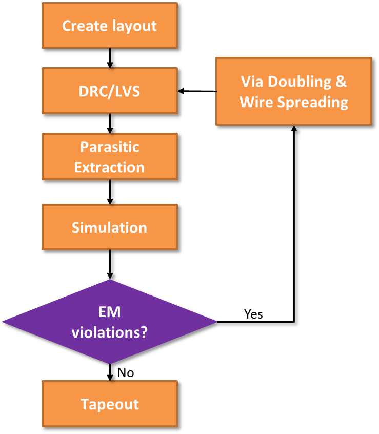
Figure 4. The EM measurement and analysis flow.
Accurate parasitic extraction calculations are essential to drive EM analysis at advanced nodes. Parasitic extraction tool functionality, such as detailed fracturing, and precise width and resistor location determination, is critical to the extraction and EM analysis process at advanced nodes.
Two tips can help designers increase the accuracy of these calculations:
1. Output the parasitic resistance width, thickness, and location
As shown in Figure 5, the designer draws a layout with the ideal width and thickness, but in reality, the width will vary due to optical proximity correction (OPC) effects, as modeled by the foundry, and the actual thickness will be different from the drawn thickness because of chemical-mechanical polishing (CMP) effects during manufacture.

Figure 5. Actual width and thickness of interconnect varies due to OPC and CMP effects during manufacturing.
Outputting the actual width and thickness creates an output netlist with accurate width parameters. Foundries include in-die variation tables in their rule decks, so when designers run the parasitic extraction tool, the actual width and actual thickness can be automatically calculated. If the actual resistance is set before the parasitic extraction tool is run, then the output netlist contains a width ($w) that takes this in-die variation (like OPC bias) into account, as shown in this netlist from a Calibre xACT 3D run:
R5 VN:6 VN:50 1.61 $w=4e-06 $l=8.05e-07 $layer=PO1 $thickness=1.3e-07
+ $X=18.8600 $Y=39.2850 $X2=18.8600 $Y2=38.4800
R6 VN:9 VN:38 0.153087 $w=5.2e-07 $l=4.35e-07 $layer=MT1 $thickness=2.5e-07
+ $X=16.9850 $Y=40.2500 $X2=17.4200 $Y2=40.2500
As shown by the equations in Figure 6, thickness and width feed into the resistance equation. To calculate an accurate resistance value to enable the simulator to calculate current accurately, it is essential to have correct width values.
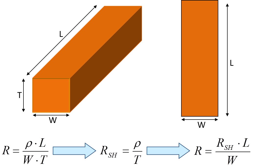
Figure 6. Width and thickness calculations can be automatically performed by parasitic extraction tools.
2. Turn Off Reduction
Reduction techniques in parasitic extraction tools are useful for decreasing simulation time. However, to run an accurate EM analysis, it is important to turn off all parasitic reduction, so the details of each interconnect segment are not lost.
In Figure 7, the interconnect was split into four segments. There is an EM violation in the narrowest segment, shown in red. If reduction is run, this segment will be combined with the other three segments, and this EM violation will be lost in the merged data.
Figure 7. To avoid losing visibility of EM violations in segments, turn off parasitic reduction.
Also, make sure no other types of reduction are specified, such as threshold or frequency-based reduction. Such reduction techniques will hide some information about resistance parameters, like resistor width, resistor layer, etc.
Turning off all reduction creates an output netlist containing each unreduced segment with its relevant width and thickness information. This output netlist can then be accurately simulated using a simulation tool with EM analysis capability.
Additional Types of EM Analysis
In addition to current density analysis for IC layouts, it is possible to have a design-context-aware interconnect reliability solution for full-chip EM analysis that considers current density, Blech Effect, and nodal hydrostatic stress analysis for failure prediction [1]. Advanced reliability solutions, such as the Calibre PERC reliability verification tool, can take the Blech Effect into consideration by measuring the longest path of the interconnect tree. If the longest path is less than the Blech length, then the current density constraint will be set to a very large value, in effect granting a waiver to that line [2].
Conclusion
EM is a significant factor in design reliability. It is important to measure EM effects in chip designs to be able to predict the MTTF, and reduce it as needed for the intended application. Parasitic extraction tools should be set up to take OPC and CMP effects into consideration, and to output accurate resistance values with accurate width parameters, to ensure accurate current density calculations.
References
[1] P. Gibson, M. Hogan and V. Sukharev, “Electromigration analysis of full-chip integrated circuits with hydrostatic stress,” 2014 IEEE International Reliability Physics Symposium, Waikoloa, HI, 2014, pp. IT.2.1-IT.2.7. doi: 10.1109/IRPS.2014.6861151
[2] D. Medhat, “Electromigration and IC Reliability Risk,” Semiconductor Manufacturing and Design Community, December 2015. http://semimd.com/favre/2015/12/10/electromigration-and-ic-reliability-risk/
Author
Karen Chow is a Technical Marketing Engineer in the Design-to-Silicon division of Mentor Graphics Corp., focusing on driving parasitic extraction development in analog and RF design flows.

Liked this article? Then try this –
White Paper: Calibre xACT Parasitic Extraction Supports Signal Integrity at Advanced Nodes
This article was originally published on www.edn.com