Not yet a fan of fan-out? Why you should be!
By John Ferguson, Mentor Graphics
FO-WLP combines multiple die from heterogeneous processes into a compact package, and that’s a good thing. Why? Here…

Fan-Out Wafer-Level Packaging (FO-WLP) is the latest buzz in the semiconductor industry. Since the announcement [1} in 2014 that TSMC was getting into the FO-WLP game with its InFO process [2], and the news [3] that they plan to use it this year in production, multi-die assembled packages finally seem to be entering the mainstream with their promise of low cost, small form factors, and low power with high performance. But what exactly is FO-WLP? How do we take advantage of it? What limitations still need to be overcome?
In its simplest form, FO-WLP is a new method for combining multiple die from heterogeneous processes into a compact package (Figure 1). It differs from the traditional silicon interposer approach in several key factors:
· While FO-WLP typically requires a silicon wafer as a carrier, it does not remain in the package. Die-to-die and die-to-ball grid array (BGA) connectivity are established through the package redistribution layers (RDL) directly.
· Because FO-WLP doesn’t require an interposer, or insertion of through-silicon vias (TSVs), costs come down. You also don’t have to worry about the unintended effects of the TSVs on electrical behavior.
· FO-WLP allows a substrate-less package, which provides a smaller vertical footprint. The shorter path to a heat sink also reduces concerns about thermal impacts.
· Thanks to the reduced vertical height gained by eliminating the substrate and the interposer, FO-WLP opens up real estate to place even more components vertically on top. This is achieved with the use of through-package vias (TPVs), which allow for package-on-package (POP) design. Unlike TSVs, TPVs act much more like the traditional vias you are used to, reducing concerns about yields and reliability. This approach is especially useful for including 3rd party DRAMs in the package.
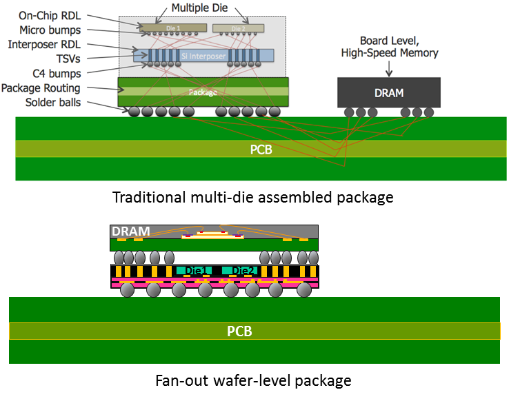
Figure 1. Fan-out wafer-level packaging can significantly reduce the package footprint.
This is not to say that FO-WLP design doesn’t present its own set of unique challenges. Historically, package design and integrated circuit (IC) design have been isolated processes. ICs are designed primarily in a Linux operating environment, using electronic design automation (EDA) tools certified by a target foundry or fab and associated with a specific process design kit. System-on-Chip (SoC) designs are typically built using primarily Manhattan geometries, and represented in gridded formats like GDSII or OASIS. When finalized, a die abstract (indicating the die’s size and the individual pin locations) is passed to a package design team using any one of several formats (LEF, AIF, etc.). When the IC design is sign-off ready, it is taped out to the foundry for manufacture.
The package design community predominantly works with EDA tools designed to run on a Microsoft Windows operating system. Packaging design uses non-Manhattan geometries extensively, and does not often map nicely to the gridded formats of the IC world. In fact, the two worlds share very few standards in terms of data representation. Package designs, along with the physical die, are historically transferred to a package house or outsourced assembly & test (OSAT) facility using a number of formats, including AIF, MCM, ODB++, and even Gerber. There is typically very little in the form of formal sign-off requirements that accompany the package design, other than a textual document describing the intended design rules.
The introduction of the FO-WLP design approach requires the communication between the IC design world and the package design world to expand beyond this limited interchange. To optimize the entire package design, IC designers must know more about the intended package, and package designers must know more about the ICs included in the package. For instance, if you want to optimize the package design for size and/or performance, then you must optimize the whole system, not just the individual elements. An IC designer might be able to design a really small IC, but in doing so, it might be more difficult to connect that die into the package, expanding the package footprint. Similarly, a package designer might be able to design a clean and tight package, while making it impossible for the IC designers to get their die I/Os to match specific locations. This is where package integrator tools can be useful (Figure 2). These types of tools allow for design co-optimization and help communicate opportunities to both sides.
Figure 2. Package integrator tools smooth the lines of communication and enable co-design optimization.
Fortunately, even though there are few common standards between the two worlds, it does not appear that new standards are required to bridge this gap. Instead, it appears that conversion between data formats may be suitable to meet the needs of all the parties involved, although we will also need tool-to-tool interfaces and communication protocols. While communicating between Microsoft Windows and Linux can be tricky, experience has shown it can be readily achieved using a virtual network connection (VNC).
The first commercially viable FO-WLP methodology is the embedded wafer-level ball grid array (eWLB) approach invented by Infineon. Infineon chose to license their approach, so it is now readily available from most of the leading OSAT providers. Of course, the cost of the license must be incorporated into the product, something OSATs must consider in their pricing strategy. However, it is very difficult for the OSATs to compete if they all use the exact same recipe.
As a result, all of the major OSATs are developing their own flavors of the FO-WLP process. Add to this the fact that TSMC has entered the game with their own InFO process, and package design companies now have a plethora of production options to choose from. Determining which offering is best for a given design requirement can be complex. In general, beyond price, product offerings are typically measured by what they can provide in terms of package footprint. Footprint is determined by the minimum vertical height that can be delivered, the minimum horizontal coverage as dictated by the minimum spacing allowed between die, and the minimum line width and space of the interconnecting redistribution layer (RDL) and BGA pitch.
With the inclusion of TSMC into the market, package designers also have a new wrinkle to configure: OSAT vs. foundry. The primary benefits touted by the foundries are 1) faster turn times due to the ability to share manufacturing lines, 2) single point of contact and one-stop-shopping, and 3) decades worth of experience in delivering full design kits together with qualified design tools. For example, TSMC is reportedly [4] employing the InFO technology in production this year, meaning they are building and validating InFO design flows, complete with required sign-off requirements, providing designers confidence that the final taped-out package will work with reasonable yields. It is likely that the OSATs will ultimately be required to follow suit in this area, putting more resources into quantifying and validating their manufacturing tolerances.
What is not likely available through TSMC or another pure play foundry would be the ability to build an assembly based on die produced by multiple foundries. It’s not likely, for example, that one would send a die manufactured at Samsung to TSMC to incorporate into an InFO package. On the one hand, using a single foundry eliminates the need to transfer die from a foundry to an OSAT, saving time and ensuring that all the information stays together from start to finish. On the other hand, choosing an OSAT places the burden of ensuring all the components work together (and debugging in the case of errors) on the package designer, to work out through multiple 3rd party partners. This choice may materially impact pricing of a full FO-WLP package, depending on a foundry’s die manufacturing offerings.
What we can say is that it appears whether you target a foundry or OSAT offering, FO-WLP is here to stay. While it does not replace all cases where a silicon interposer is required, it enables a new design methodology with several key advantages that package designers will likely want to take advantage of. You can expect FO-WLP to be a continued area of growth over the next several years, as 3D IC technologies continue to expand.
References
[1] www.tsmc.com/download/ir/annualReports/2014/english/pdf/e_1_1.pdf
[2] ieeexplore.ieee.org/stamp/stamp.jsp?arnumber=6479039
[3] www.appliedmaterials.com/nanochip/nanochip-fab-solutions/december-2015/fan-out-is-a-game-changer
[4] www.macrumors.com/2015/11/06/tsmc-a10-production-info-wlp/
Author
John Ferguson is the Director of Marketing for Calibre DRC Applications at Mentor Graphics in Wilsonville, Oregon, and has extensive experience in the area of physical design verification.

This article was originally published on chipscalereview.com