Parasitic extraction for touchscreen designs
By Mohamed ElRefaee, Mentor Graphics
Accurate parasitic extraction of touchscreens is essential for ensuring the high-quality performance the market demands

The popularity of touchscreens is growing rapidly as they become an integral part of smartphones, tablets, automobiles, and even consumer appliances. Touchscreens remove the need for peripheral elements, such as a mouse or keyboard, enabling electronics to become more portable and lightweight, and allowing developers to increase the size of the display screen in the device. Based on a recent report published by IHS, the touch panel market is forecast to grow to about 2.1 billion units in 2015, up 15.1% year-over-year, and reaching 2.8 billion units in 2018 [1].
A touchscreen detects and locates the touch of a human finger or a passive object, such as a stylus, over a display area. There are many types of touchscreens, but the main categories are:
- Capacitive
- Resistive
- Surface Acoustic Wave
- Infrared
Because capacitive touchscreens are the most common type being used today, especially in smartphones, I’ll use this type as my example. Capacitive touchscreens consist of an insulator such as glass, coated with a transparent conductor such as indium tin oxide (ITO) and containing an embedded array of capacitors that form a matrix. Because a human body is an electrical conductor, touching the surface of a touchscreen distorts the electrostatic field, measured as a change in the mutual capacitance between transmitting and receiving electrodes embedded in the touchscreen. Touch tools, such as a capacitive stylus or gloves that include conductive thread, may also be used. In the absence of any external stimulus, the capacitance values of the elements of the array should all be equal, except for the elements at the extremities of the screen, which are subject to boundary variations.
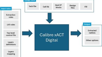
One of the major verification challenges for touchscreens is parasitic extraction. Because a finger or touch tool is essentially a big conductor sitting on top of the screen, a 3D field solver extraction tool is typically required to achieve the desired accuracy necessary to capture the subtle effect at the touch point. However, most field solvers do not have the capacity to evaluate an entire design in a timely manner, making them unacceptable for production design.
Capacity in this instance means the ability of the extraction tool to run on big designs to completion. For example, if an extraction tool runs on a design for three days and generates accurate results, it does not suffer from a capacity issue, but it may suffer from a performance issue. If another extraction tool runs on that same design, but never finishes, it has a capacity issue, which means the algorithm inside the tool is not well-suited for large designs. Capacity is simply a metric, like accuracy and performance. With field solvers, capacity is typically an issue because of the resources required to do the extensive computational work. What is needed is an extraction tool that can deliver field solver accuracy with a satisfactory turnaround time for production designs.
Extraction Techniques for Touchscreens
Once the layout of the capacitor array is defined, a parasitic extraction tool is used to calculate the capacitances from the physical dimensions to verify that the design will operate as expected. These types of designs are based on a pattern that is repeated all over the screen. Therefore, selecting a subset of the array from any part of the screen other than the extremities will provide an adequate representative of the full screen. When selecting a sub-array, the bigger the array is, the better, because the effect of the boundary perturbation is not dominant around the middle of the array, and the results will be more credible. A designer could run extraction on the full screen if desired, but that would incur a very long runtime, and is not usually needed in initial testing.
I’ll walk through an example using the Mentor Graphics Calibre xACT 3D extraction tool, part of the Calibre xACT extraction platform. The Calibre xACT 3D tool uses a combined finite and boundary element method (FEM/BEM) [2] [3] [4], with a very efficient algorithm that not only computes quickly, but also allows the job to be distributed to multiple CPUs for faster overall runtime without losing the fundamental accuracy of the FEM/BEM technique.
To characterize a full screen, a small sub-array is extracted and the results are extrapolated to represent the full screen. In the 5 by 5 array shown in Figure 1, each crossover point between each x and y node represents a capacitance to be measured.
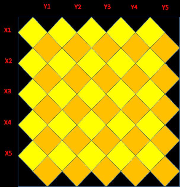
Figure 1 A 5 x 5 array of capacitors representing a portion of a touchscreen display
The extraction tool computes all the capacitances in the matrix which, if plotted in a 3D graph, looks similar to the graph in Figure 2. Ideally, the plane of this matrix is very flat, which is crucial to minimizing errors when the finger touch or stylus is employed. The field solver solves for the electric potential in a window that has a mesh of points. While the window size cannot be controlled by the user, the density of the points inside that window can be specified. To ensure that the flatness of the plane is indeed characteristic of the panel design, we use the highest-accuracy mode in Calibre xACT 3D to force the solver to solve in more points inside the window, yielding more accurate results.
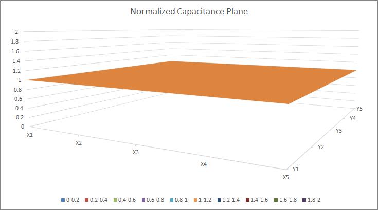
Figure 2 Extracted capacitance values across a touchscreen matrix
A change in the measured capacitance at the touch point is seen when a touch tool is used. There is an electromagnetic field between conductors, due to the charges accumulated on them. These field lines go from one conductor to the other. If a third conductor (like a stylus) is present, some of those lines will terminate on that new conductor. This effect is called shielding, and results in a reduced coupling capacitance between the original two conductors. When the touch tool is placed at the X3Y3 node, the capacitance at that point goes down, due to the shielding effect of the touch tool, as shown in Figure 3.
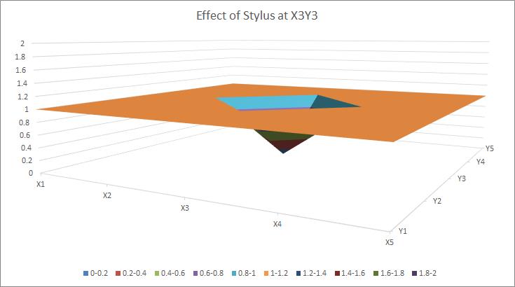
Figure 3 Change in measured capacitance at touch point
The magnitude of the dip at the touch point depends on several factors, including the stylus size and model, among others. This capacitance change is what the circuit uses to detect the stylus position. The bigger the dip, the easier it is to detect. Optimally, the capacitance should be equal (or almost equal) over the entire array, except for the touch point and its neighboring points. The biggest dip should be seen at the touch point, with smaller dips around the near points. A bad result would be when the designer sees no change in the capacitance at the touch point, or a very small change that cannot be detected by circuitry. One way to improve unacceptable results is by changing how the stylus is modeled.
Touchscreens are becoming a ubiquitous part of the electronics landscape. With the right tools and the right techniques, designers can ensure that their touchscreen designs will deliver the performance the market requires, while also ensuring they deliver their products to that market in a timely manner.

Liked this article? Then try this –
White Paper: The Calibre xACT Platform: Next-generation parasitic extraction for 16nm and beyond
This article was originally published on www.edn.com