Parasitic Extraction of FinFET-based Memory Cells
By Karen Chow, Mentor Graphics
Accurate and efficient FinFET characterization requires a parasitic extraction tool that can apply different extraction methods to analyze the full range of parasitic conditions quickly and precisely throughout the design cycle.

Memory chips must meet strict specifications for fast data transfer, reliability, and power consumption, so accurate characterization is required at every stage of design.
The introduction of FinFETs at 16 and 14 nm nodes enables higher density and performance, and reduced power usage, but it also increases challenges in design and validation. Memory designers need a tool that can help them analyze parasitics quickly and accurately throughout the design cycle.
Introduction to FinFETs
FinFETs are three dimensional structures that rise above the substrate and look like a fin, hence the name. Theses fins form the source and the drain, and the gate wraps around the source and drain, providing better control of the channel.
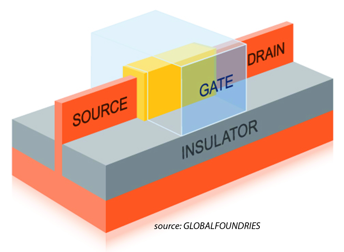
When the device is in the off state, there is very little leakage current. With FinFET designs, there is low threshold voltage, and a lower supply voltage can be used. This drop in supply voltage results in reduced power usage while maintaining performance.
Parasitic resistance and capacitance of FinFETs
With FinFET structures, it is important to accurately capture the parasitic resistance and capacitance within the device, as well as inter-device interactions. Also, some foundries model floating devices in between the designed FinFETs, and it is important to capture the coupling to the floating devices, as well as coupling between the main designed devices.
When extracting FinFETs, it is important to capture the coupling to floating devices, as well as coupling between the main designed devices.
Parasitic resistance is also important. As the fin channel and the source drain regions narrow, increased source drain resistance degrades the performance of the devices. The source/drain resistance is composed of spreading, sheet and contact resistance, and is around 150 ohms for p-type FinFETs, and 116 ohms for n-type FinFETs, with gate overdrive voltage between 0.6 and 1.2V [1].
The parasitic capacitance and resistance within and between FinFETs can be modeled either by the parasitic extraction tool, or in the device model used for simulation. It is important to ensure that there is no double counting of effects, and no missing effects, in the boundary between extraction tool and device model. The trend for smaller nodes is to have the parasitic tool do more of the modeling, since it can take the layout-dependent effects into consideration.
Flat vs. hierarchical extraction
When doing parasitic extraction with FinFETs, flat extraction is often done since it allows all coupling effects to be taken into consideration. But sometimes, the runtime of a flat extraction can be too long. Hierarchical extraction can be done to reduce runtime. In hierarchical extraction, each level of the hierarchy is extracted in isolation, and then each level of hierarchy is stitched together. The upper levels of hierarchy can see coupling capacitance effects into lower levels of hierarchy, but then the coupling is grounded. This is called a “grey box” flow.
Boundary condition extraction
An alternate approach is to apply boundary conditions on a single cell. Extraction using boundary conditions enables the extraction of an isolated cell by simulating the parasitic effects of neighboring conductors, either by reflecting the boundaries, or by virtually placing the same block repeatedly. The illustration below shows an example with both reflective and periodic boundaries. A reflective boundary is equivalent to placing a reflective wall at the boundary, and placing a mirror image of the cell on the other side of the wall. A periodic boundary replicates the enclosed geometries, creating copies on the other side of the boundary. The upper left corner of the figure shows a cell extracted in isolation, where the y direction is periodic, and the x direction is reflective. The larger diagram on the right shows an entire array of cells as a flat extraction. Extracting just a single cell, but reflecting the boundaries can provide almost the same accuracy as running a flat extraction, with significant runtime advantages. This boundary condition methodology works well for memories, because identical structures are repeated over and over again.

A boundary condition extraction technique works well for memories, because identical structures are repeated over and over again.
Using a field solver for extraction of memory designs
For memory designs, the bit cell is usually defined first, and it can be extracted and simulated in isolation. Then, boundary condition extraction can be used to determine how the neighborhood will affect the performance of the bit cell. In the extraction process for memories, every stage of design verification can benefit from field solver accuracy.
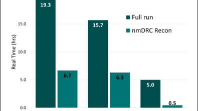
Table 1 compares the extraction runtime required for a 16 nm memory design using the boundary condition technique and traditional extraction of the full 4×8 array, and a 1M instance. In each case, we used the Calibre xACT 3D field solver extraction tool, which provides high accuracy but employs efficient parallelization techniques to optimize multi-CPU runtime performance.
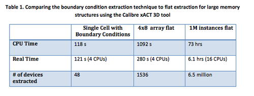
Running a single cell with boundary conditions versus a flat 4×8 run provides a runtime improvement of 9.2X. For much larger memory blocks, there is a proportionally greater advantage to using this methodology. The runtime of a rule-based extraction tool is expected to be similar to a single cell run with boundary conditions, although much less accurate. Flat extraction of all 1M instances (6.5 million devices) provides the highest accuracy with a runtime of 6.1 hrs using 16 CPUs, which reflects a highly scalable field solver performance supporting overnight turnaround.
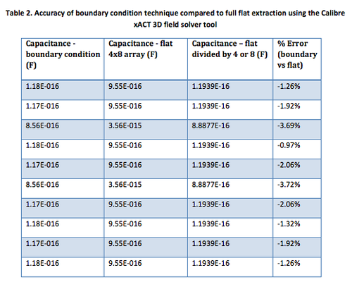
There is some accuracy degradation when using the boundary condition method vs. extracting the whole block flat. Capacitance of the single cell was compared with the full 4×8 array with the capacitance divided by either 4 or 8 depending on whether the line was going in a horizontal or vertical direction). The accuracy degradation due to the isolation of a single cell is shown in Table 2 below.
Running flat parasitic extraction with a field solver is always the most accurate solution, but other good alternatives include running a cell or subset array using boundary conditions, or running with a rule-based extraction tool. A rule-based extraction tool can be used during the iterative design cycle, when quick turn-around times are required, and a field solver can be used for bit cell design and final sign-off, ensuring the highest accuracy possible.
Conclusion
Using a field solver for extraction during all phases of a memory design, from bit cell design, to block characterization, to full chip sign-off ensures that the chip will work to specification when it is manufactured. The boundary condition extraction technique can reduce field solver runtime by orders of magnitude with only minor accuracy degradation on the order of 1-4 percent compared to full flat extraction.
References
[1] Yoon, Jun-Sik, et al. “Extraction of source/drain resistivity parameters optimized for double-gate FinFETs.” Japanese Journal of Applied Physics 54.4S (2015): 04DC06.
Author
Karen Chow is a technical marketing engineer in the Design-to-Silicon division of Mentor Graphics Corp. in Wilsonville, Oregon, focusing on driving parasitic extraction development in analog and RF design flows. Prior to joining Mentor Graphics, Karen worked in the telecommunications and EDA industries, designing analog ICs and supporting EDA tool development. She received her Bachelor of Science degree in electrical engineering from the University of Calgary, and her MBA from Marylhurst University.

Liked this article? Then try this –
White Paper: The Calibre xACT Platform: Next-generation parasitic extraction for 16nm and beyond
Testimonial: Cypress Semiconductor Testimonial
This article was originally published on www.eetimes.com

Comments
Leave a Reply
You must be logged in to post a comment.
nice article, but on which base 150 ohms for p-type and 116 ohms for n-type is selecting? if we reduce the resistance below that can we achieve better performance?