Part 6: The 2010 Wilson Research Group Functional Verification Study
Testbench Characteristics and Simulation Strategies
This blog is a continuation of a series of blogs that present the highlights from the 2010 Wilson Research Group Functional Verification Study.
In my previous blog, I focused on the controversial topic of effort spent in verification. In this blog, I focus on some of the 2010 Wilson Research Group findings related to testbench characteristics and simulation strategies. Although I am shifting the focus away from verification effort, I believe that the data I present in this blog is related to the discussion of overall effort and really needs to be considered.
Time spent in top-level simulation
Let’s begin by examining the percentage of time a project spends in top-level simulation today. Figure 1 compares the time spent in top-level simulation between FPGA designs (in grey) and non-FPGA designs (in green) from our recent study.
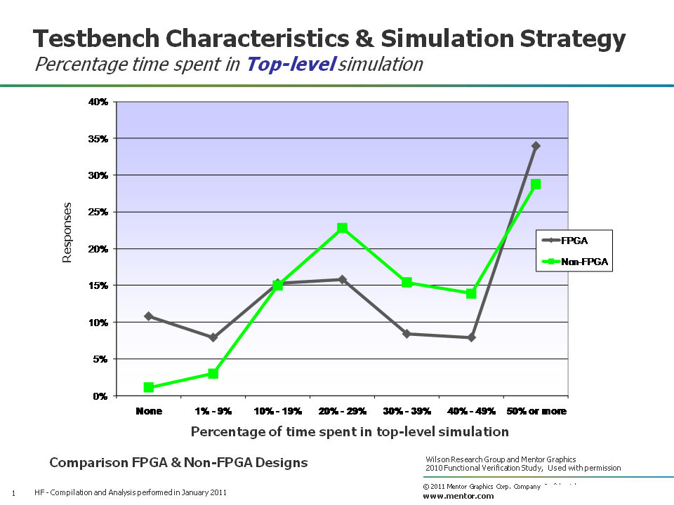
Figure 1. Percentage time spent in top-level simulation
Obviously, the study results show that projects are all over the spectrum, where some projects spend less time in top-level simulation, while others spent much more time.
I decided to partition the data by design size (using the same partition that I’ve presented in previous blogs), and then compare the time spent in top-level verification by design size for Non-FPGA designs. Figure 2 shows the results, where the design size partitions are represented as: less than 1M gates (in blue), 1M to 20M gates (in orange), and greater than 20M gates (in red).
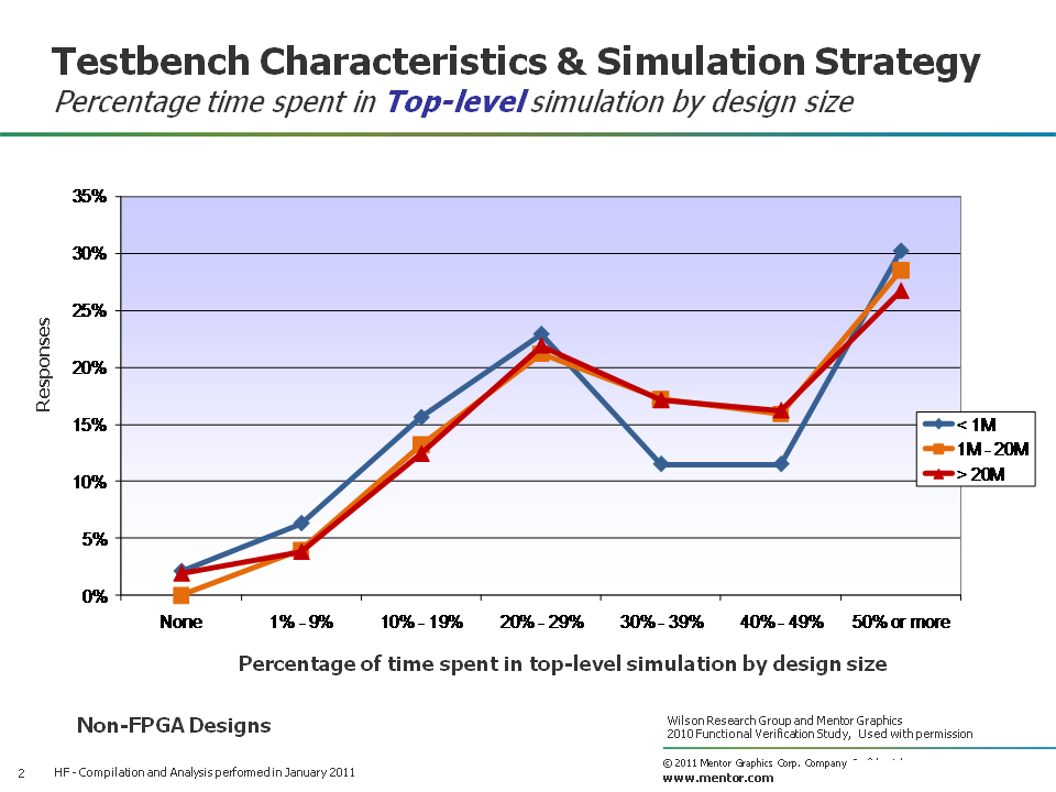
Figure 2. Percentage of time spent in top-level simulation by design size
You can see from the results that, unlike previous analysis where the data was partitioned by design size, it didn’t seem to matter for design sizes between 1M-20M gates and design sizes greater than 20M gates. That is, they seem to spend about the same amount of time in top-level verification.
Time spent in subsystem-level simulation
Next, let’s look at the percentage of time that a project spends in subsystem-level simulation (e.g., clusters, blocks, etc.). Figure 3 compares the time spent in subsystem-level simulation between FPGA designs (in grey) and non-FPGA designs (in green) from our recent study.
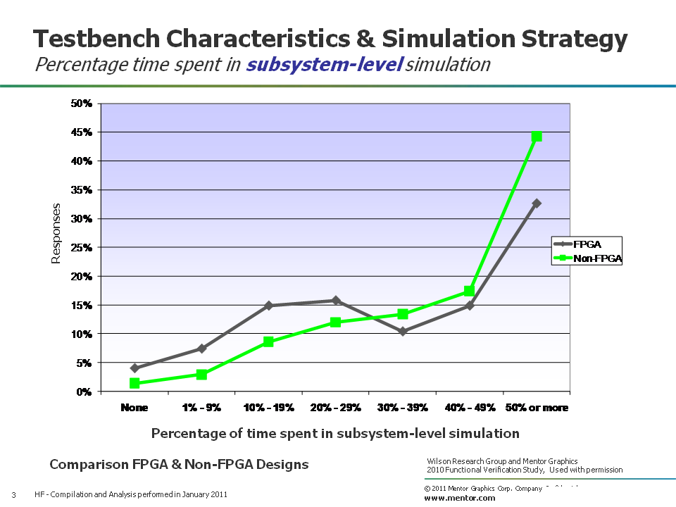
Figure 3. Percentage of time spent in subsystem-level simulation
Non-FPGA designs seem to spend more time in subsystem-level simulation when compared to FPGA designs. Again, this is probably not too surprising to anyone familiar with traditional FPGA development. Although, as the size and complexity of FPGA designs continue to increase, I suspect we will see more subsystem-level verification. Unfortunately, we can’t present the trends on FPGA designs, as I mentioned in the background blog for the Wilson Research Group Functional Verification Study. However, future studies should be able to leverage the data we collected in the Wilson Research Group study and present FPGA trends.
Figure 4 shows the Non-FPGA results for the time spent in subsystem-level verification, where the data was partitioned by design size: less than 1M gates (in blue), 1M to 20M gates (in orange), and greater than 20M gates (in red). There doesn’t appear to be any big surprise when viewing the data with this partition.
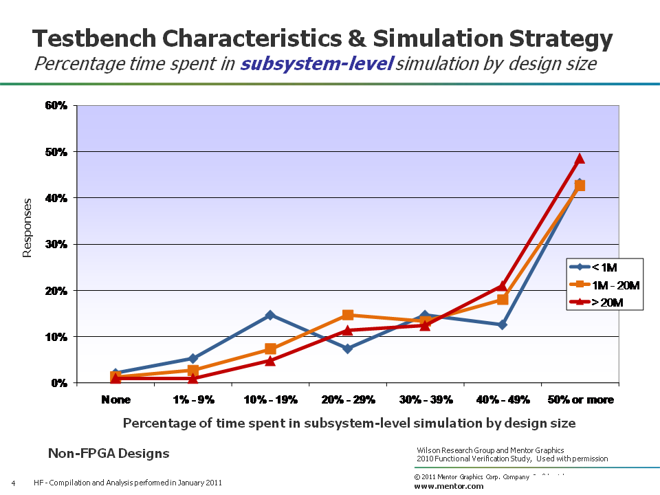
Figure 4. Percentage of time spent in subsystem-level simulation by design size
Number of tests created to verify the design in simulation
Now let’s look at the percentage of projects in terms of the number of tests they create to verify a design using simulation. Figure 5 compares the number of tests created to verify a design between FPGA designs (in grey) and non-FPGA designs (in green) from our recent study.
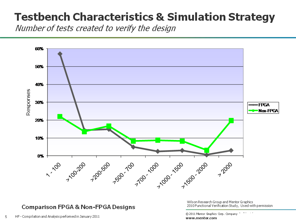
Figure 5. Number of tests created to verify a design in simulation
Again, the data is not too surprising. We see that engineers working on FPGA designs tend to create fewer tests to verify their design in simulation.
Figure 6 shows the trend in terms of the number of tests created to verify a design in simulation by comparing the 2007 Far West Research study (in blue) with the 2010 Wilson Research Group study (in green). You will note that there has been an increase in the number of tests in the last three years. In fact, although there is a wide variation in the number of tests created by a project, the median calculation trend has grown from 342 to 398 tests.
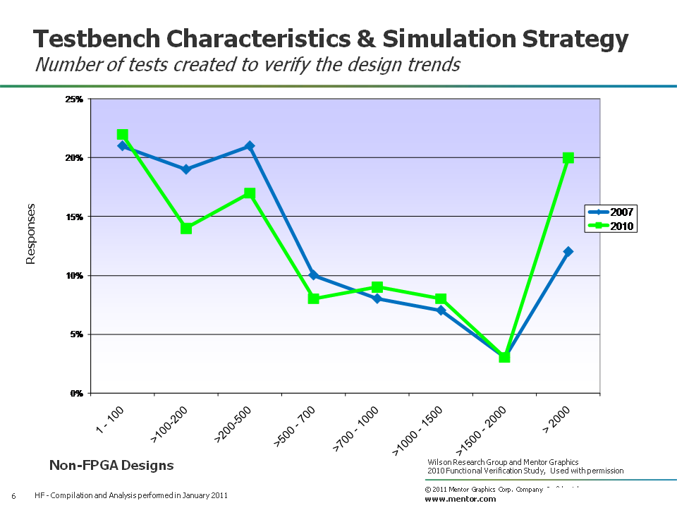
Figure 6. Number of tests created to verify a design in simulation trends
I also did a regional analysis of the number of tests a non-FPGA project creates to verify a design in simulation, and the median results are shown in Figure 7, where North America (in blue), Europe/Israel (in green), Asia (in yellow), and India (in red). You can see that the median calculation is higher in Asia and Indian than North America and Europe/Israel.
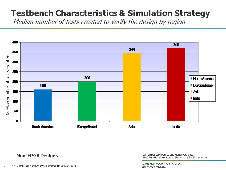
Figure 7. Number of tests created to verify a design in simulation by region
Finally, I did a design size analysis of the number of tests a non-FPGA project creates to verify a design in simulation, and the median results are shown in Figure 8, where the design size partitions are represented as: less than 1M gates (in blue), 1M to 20M gates (in orange), and greater than 20M gates (in red).
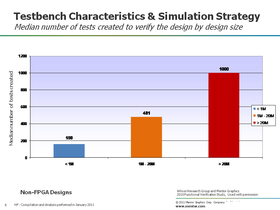
Figure 8. Number of tests created to verify a design in simulation by design size
Obviously, larger designs require more tests to verify them in simulation.
In my next blog, I’ll continue focusing on testbench characteristics and simulation strategies, and I’ll present additional data from the 2010 Wilson Research Group study.


Comments