Webinar: How to implement DFT in 2.5/3D designs using Tessent Test software
In the era of more-than-Moore’s law, chip makers are scaling by adopting complex architectures that connect dies vertically (3D IC) or side-by-side (2.5D). There has been progress throughout the semiconductor ecosystem in bringing 2.5D and 3D ICs designs to the mainstream, including design-for-test (DFT).
If you are an engineer, DFT manager, CAD director or someone investigating DFT for 2.5D/3D IC design, register for this free webinar to learn about how the new Tessent Multi-die software automates the complex DFT tasks associated with 2.5D and 3D IC designs.
Title: Implementing DFT in 2.5/3D designs using Tessent Multi-die software
Date: Available On-Demand
Duration: 1 hour
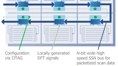
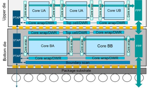
Tessent Multi-die software automates the generation and insertion of IEEE 1838 compliant hardware, defining the IEEE test access architecture for three-dimensionally stacked or 2.5D side-by-side integrated circuits. This solution helps customers dramatically speed up and simplify critical DFT tasks for next-generation ICs based on these architectures.
What you will learn in this 3D IC test webinar:
- How Tessent Multi-die supports the IEEE 1838 standard, including how Tessent Streaming Scan Network (SSN) can be used as the Flexible Parallel Port (FPP) for the standard
- How Tessent tools can help with DFT implementation for 2.5D/3D ICs
- How interconnect boundary scan-based patterns between the dies can be extracted using Boundary Scan Description Language (BSDL) from individual dies for 2.5D designs. Plus, unified package level BSDL creation in both 2.5D/3D devices
- How IJTAG complements both 2.5D and 3D test