Efficient and effective DFT for 3D stacked die

3D devices are coming, and we are ready.
When existing advanced 2D designs already push the limits of design-for-test (DFT) tools, what hope do developers have of managing DFT for 3D devices? Can anyone afford the tool run time, on-chip area demand, pattern count, and test time? The answer, from an array of experts, is yes, there is a path to a scalable, affordable, and comprehensive DFT solution for 3D ICs.
Read details in our technical paper.
Well-covered strategies include using high-quality known-good-die (KGD) testing for dies that will be assembled in a 3D stack. KGD test usually includes all package tests, except the interconnect tests between dies. The new and tricky parts include the stack, so let’s discuss that.
In many ways, a 3D DFT solution is an extension of the hierarchical DFT principle common in industry. There’s just one more level of hierarchy to consider, the stack level.
About IEEE 1838
Test standards provide the foundation of interoperability between the entire ecosystem involved in the development of a product. IEEE 1838-2019 standardizes the test access for 3D stacked die designs. Figure 1 illustrates an IEEE 1838-2019 schematic overview.
The standard adds a few new hardware pieces:
- A primary TAP (PTAP) – Basically an 1149.1 TAP with a 3D configuration register (3DCR).
- Secondary TAPs (STAP) – Each STAP talks to the PTAP of another die. They are controlled by the 3DCR and together make up the Serial Test Access (STA) network.
- Die Wrapper Register (DWR) – For wrapping each die. Only the die connected to the outside has a classic boundary scan register description. Dies can also have a boundary scan chain.
- The Flexible Parallel Port (FPP) – Optional component to carry scan-ATPG patterns through multiple dies to the target die. It can be configured in different ways through the PTAP.
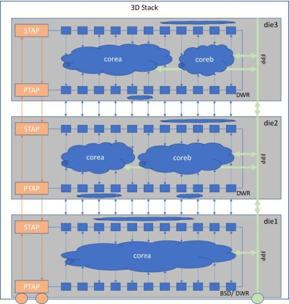
The components from IEEE 1838 enable die-level test within the 3D stack of dies. You have to configure the hierarchy of PTAPs and STAPs to enable access to the FPP for scan-ATPG (or to the IJTAG network for BIST) of the target die.
Using IEEE 1838 to move test data
Implementing the 1838 TAPs and the IJTAG-based network
IEEE 1838 does not provide a hardware description language, but you can model the (P/S)TAPs in IJTAG. The rest of the die-internal IJTAG network and instruments, like LBIST and MBIST IPs, are implemented, inserted, and connected in the usual way of 2D, just using the PTAP as the network source, instead of the 1149.1 TAP.
Implementing the FPP
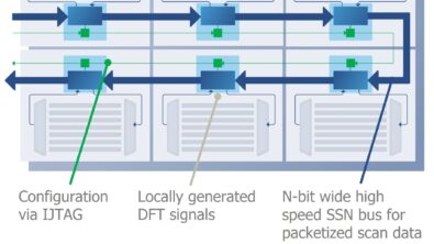
You can use Tessent Streaming Scan Network (SSN) to implement the FPP. The SSN network can meet the data transfer demand of each target core, and even be configured to use broadcasting, in which multiple hosts receive the same data and each core’s pass/fail can be observed. We expect that in a 3D configuration with many identical die/chiplets, broadcasting will save a lot of time.
The expansion of the SSN network from 2D to 3D is straightforward. There is no change in the hierarchical scan-ATPG pattern generation. The patterns are still computed at the core level and mapped to the SSN bus. In a 3D architecture, the bus now connects dies; the bus network only sees more cores.
With this expansion, high-volume data, like the scan-ATPG test patterns or diagnosis patterns, can be applied to any number of cores in any number of dies in the stack simultaneously. The ability of a human to do this is already very limited in 2D. In a 3D configuration, this can only be done through tool automation.
Wafer-level test
What about scan-ATPG patterns at the wafer level, where there is no stacked-dies SSN network?
To answer this question, let’s look at the SSN schematic (figure 2). The multiplexor in the middle, lower core enables a short return path for the bus. In the 3D configuration, such muxes are used to temporarily ‘loop back’ the up signals to the down-signals. This means that the SSN network implemented in each die for 1838 purposes can also be used for wafer-level testing. The very same core-level, scan ATPG patterns, computed once, will be mapped twice, once to the SSN network of the die for wafer-level testing, and one time to the SSN network of the stack for final package-level testing.
What if there is no physically accessible way to apply die-level patterns at the wafer level? One solution is to use sacrificial pads, i.e. pads that are only available at the wafer level. These pads can be contacted as usual allowing the application of wafer-level tests, even though in a stacked configuration the signal would physically go through a through-silicon via (TSV).
Die-to-die testing
What about die-to-die testing in a 3D stack? The most universal test would be to deploy ATPG between the dies, especially if there is logic between the DWR and the die IOs.
One way is to upgrade all die-to-die IOs to bidirectional signals and IOs, where an internal loop-back can be used to determine for example shorts (leakage) in the connectivity. This test extends to the stack level. A BIST engine controlled by the IJTAG implements the test. Another way is to use the emerging 2.5D die-to-die interconnect standards, like Universal Chiplet Interconnect Express (UCIe), which includes interconnect test as well as lane repair as part of the standard.
Managing data volume
Still, this is a lot of data for an EDA tool to handle, right? Indeed. Which is why using ‘gray box’ strategies is essential. Gray boxing describes the creation of a stripped-down version of cores, usually only consisting of wrapper chains and the logic between the chain and the core’s IO.
The same concept of core gray boxing transfers directly to dies. The die-level gray boxing takes the wrapper chains and any logic in between the chains and the die’s IOs so the tools can load all needed gray box design views and deploy any die-to-die testing. Further, it allows Verilog simulators to validate the die-to-die patterns by only loading the gray box views of all relevant dies.
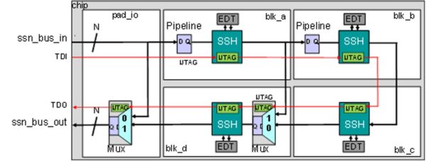
But we also need to use “IJTAG gray boxing.” An example is shown in figure 3. Say you want to generate patterns for an MBIST controller in the left instance of corea in the top left die. All you need is the ICL network and the instrument ICL and PDL. For Verilog simulation of the MBIST patterns at the core level, the RTL of corea is sufficient. At the die-level, all clock path timing from the parent of the corea instance comes into play, for example, for at-speed testing for both logic and memories.
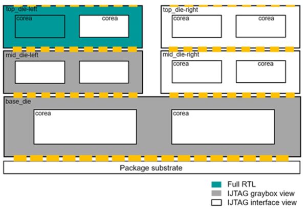
For Verilog simulation at the stack level, however, you need to load the RTL of multiple dies simultaneously to perform stack-level RTL simulation of any of your patterns. The IJTAG gray box generates an RTL version of the dies that contains only the elements of the IJTAG network needed for simulation. In figure 3, this would be the IJTAG gray box for the bottom and the middle die and only the RTL of the top left die. There are IJTAG white boxes, which are only the interface view (i.e. no body), for all IJTAG blocks and cores not on the path to the destination instrument further reducing the RTL demand to be loaded.
The same solution applies to ATPG. Any efficiently implemented solution for stacked die DFT depends on some form of white and gray boxing that is automated by the software tools.
Summary
The crucial aspect of a 3D DFT solution is tool automation and ease-of-use. In 3D, it is no longer possible for a DFT engineer to oversee all components and patterns, or even load the RTL for the entire stack. Tool automation must support the DFT engineer throughout the entire flow. Automated gray and white boxing for ATPG and IJTAG becomes the pivotal element for an affordable, overall solution of a hierarchical 3D DFT flow. DFT for 3D stacked die devices is not only possible with known technologies but is affordable and scalable.
Read details in our technical paper.
The work summarized in this paper reflects contribution from the following people: Jean-François Côté, Jeff Fan, Sean Shen, Givargis Danialy, Marcin Lipinski, Michael Garbers, Martin Keim, Vidya Neerkundar, Andreas Glowatz, Joe Reynick, Ayush Patel, and Joanna Michna.