Webinar: Memory test using a shared bus Interface
The explosive growth in the use of memory content on SoCs calls for a new solution to effectively access the memories for testing.
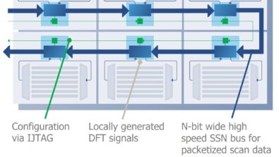
One solution is to use a shared bus architecture. This memory architecture allows for testing and repairing memories within IP cores through a single access point. This common access point for multiple memories has two big advantages:
- It allows users to optimize routing and core performance.
- It introduces flexibility for handling design-for-test (DFT) signals along functional paths behind the shared bus interface.
Tessent MemoryBIST instruments automatically hook to the DFT signals to apply MBIST patterns through the shared bus interface. In addition, Tessent MemoryBIST provides an automated approach called shared bus learning to map the physical memory composition of each logical memory and to validate the cluster and logical memory library files.
To learn more about the shared bus architecture and how the out-of-the-box solution from Tessent MemoryBIST facilitates memory testing using a shared bus interface, watch our on-demand webinar.
This webinar covers:
- The basics of a shared bus architecture overview and how Tessent supports it
- What’s needed to map and validate memory library files
- Details of the Tessent MemoryBIST test flow
- How to handle repairable memories in a memory cluster module
- Available support for multi-port and complex memory configurations
- Using the Tessent DFT solution to optimize chip performance with minimal area and design changes
Register to learn more how Tessent MemoryBIST makes it easy to use a shared bus interface to test multiple memories.