Achieving manufacturing excellence in 3D IC design
The semiconductor industry is undergoing a pivotal evolution, fueled by the adoption of 3D IC and innovative packaging technologies. Achieving manufacturing excellence in this complex landscape is not just an option but a necessity for companies aiming to lead in technology and operational efficiency.
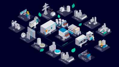
Streamlining 3D IC design to manufacturing
Siemens provides a suite of solutions aimed at streamlining the design, verification, and manufacturing processes of advanced semiconductor products.
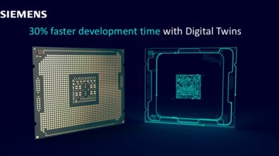
Integrated tools: Accelerating innovation in IC design through integrated design, IP, and data management tools, which significantly boost productivity and enable IP reuse.
3D IC success: A holistic design cockpit for successful planning, integration, and verification of 2.5D and 3D ICs ensuring seamless transitions and high-quality output.
Excellence in manufacturing: Advanced manufacturing planning and yield optimization are crucial for seamless production handoff, which significantly enhances the production timeline and cost-effectiveness.
Key components for manufacturing excellence
Excellence in manufacturing requires more than just advanced tools; it needs a strategic approach to integration and execution:
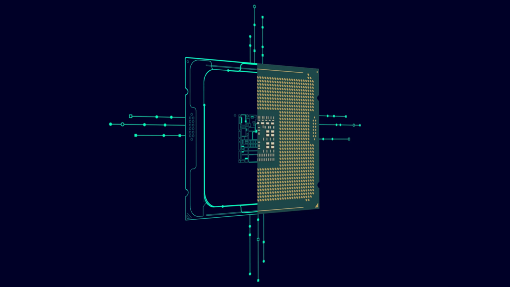
- Multi-physics and DFM analysis: Performing multi-physics and design for manufacturability (DFM) analysis is essential for creating high-density semiconductor packages that meet electrical compliance and manufacturability standards.
- Integrated Product Lifecycle Management (PLM) solutions: Connecting BOM (bill of materials) with BOP (bill of process) through integrated PLM solutions ensures that manufacturing is streamlined, yielding higher product quality and reducing costs.
- Early validation and traceability: Validating designs at early stages and maintaining traceability from design to manufacturing are critical for addressing potential manufacturing issues upfront, thereby improving yields and reducing overall costs.
- Sustainability and compliance: Embracing sustainable and compliant manufacturing practices ensures that the industry remains future-proof, focusing on material compliance and energy-efficient processes.
Future-proofing the semiconductor industry
The need for integrated, software-centric solutions in the semiconductor industry is more pressing than ever. These solutions not only facilitate entry into new markets but also enable the production of flexible, intelligent products. By leveraging Siemens’ comprehensive approach to 3D IC design and manufacturing, companies can significantly boost their time-to-market, ensure product quality, and achieve cost efficiency—all while adhering to sustainable, compliant manufacturing practices.
Summary
Advancing 3D IC design and manufacturing excellence involves a robust combination of innovative technology, strategic process integration, and a focus on sustainability and compliance. Siemens continues to be at the forefront, providing the tools and strategies necessary for semiconductor companies to excel in this challenging yet rewarding field.
Explore our 3D IC design solutions to help you achieve faster time-to-market for semiconductor products.