Leverage EDA data without conversion to generate PCB simulation models and calculation meshes
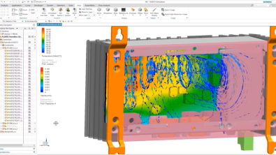
Remaining competitive in developing reliable electronics requires an innovative and adaptive engineering approach. Predicting product physical performance influences and reliability earlier in development is essential, leading development teams to leverage simulation and testing. Using Smart PCB with material map technology enables design insight based on printed circuit board (PCB) modeling reliability in less time.
Simulating Multiphysics phenomena on the printed circuit board (PCB) with Smart PCB
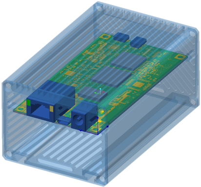
Smart PCB is a unique approach to simulate multiphysics phenomena on the printed circuit board considering all nets with the maximum level of detail. Engineers can generate simulation models and calculation meshes using electronic design automation (EDA) data. Without the need to convert EDA into a CAD model explicitly, the result is a simple-but-complete models.
Smart PCB can simulate:
- Conduction with free or forced convection, radiation
- Conduction coupled with HyperLynx DC Drop Simulation
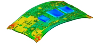
- Structural analysis (standalone or coupled)
The Smart PCB Finite Element Method (FEM) model allows for accurate and time-effective stress analysis of a PCB. It uses the PCB’s internal structure details from an original EDA file without creating the explicit geometry in CAD.
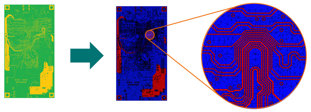
Using EDA data for automatic generation of a mesh for conduction and structural analysis
As mentioned, Smart PCB generates a FEM mesh for conduction and structural analysis automatically from EDA data. The FEM mesh is constructed from two-dimensional triangles extruded to the third dimension. Each layer is built independently and the resulting layer meshes are in glue contact with each other.
Benefits of this technology and approach include:
- Automatic hex-dominant mesh: Provides accurate simulation of problems in which bending deformations dominate on relatively coarse meshes due to minimizing the number of tetrahedral elements.
- Auto glue contact: Minimizes the calculation time of projects with many glued surfaces without specifying the contact surfaces manually.
- All-in-one: Direct integration of the structural analysis module and the computational fluid dynamics (CFD) module allows engineers to carry out complicated simulations for structural analysis by using the results of a CFD analysis calculation automatically, avoiding conversion of CFD results to external finite element analysis (FEA) software.
- Smart PCB FEM: Unique technology of structural analysis for PCBs based on the Smart PCB technology enables engineers to perform static and thermal analyses on multilayer boards. The analysis considers the traces and via layouts without the need to have them added as solid geometry in CAD.
Learn more about accelerating the thermal to structural workflow in this on-demand webinar.