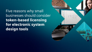
Electronic Design Automation (EDA) sits at the heart of every electronics innovation. Yet for many engineers, onboarding onto an advanced…
he Xpedition product family has introduced token-based add-on licensing; a tailored approach designed to maximize efficiency and savings, catering specifically to the dynamic needs of small businesses.
Remote collaboration in ESD is no longer a stopgap nor isn’t just feasible. It’s a strategic shift. It’s a smarter, scalable way to build the future.
In season three of the Printed Circuit Podcast, host Steph Chavez sat down with Per Viklund, Director of IC Packaging…
In a season three of the Printed Circuit Podcast, host Steph Chavez welcomed industry expert Tara Dunn, Director of Training…
What if your design team could cut development time in half while improving product quality? In today’s fast-paced electronics industry, the ability to optimize time-to-market isn’t just convenient—it’s essential for survival and success.
Previously on episode 24 of the Printed Circuit Podcast, host Steph Chavez brought together two seasoned experts—Max Clark, Product Strategy…
Previously on the premiere episode of Season 3 of the Printed Circuit Podcast, host Steph Chavez sat down with John…
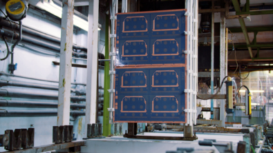
PCB material discussions are often focused around stackup material selection. These tend to be framed by questions like: ‘We use material ‘x’ for our designs and really like it. What do you think of it?’ This often veils the real question which is: ‘Do you know a good alternative to it?’