PCB high voltage spacing: What every engineer should know

As modern electronics continue to push the boundaries of power and performance, high-voltage systems are becoming increasingly common in applications like electric vehicles, industrial automation, renewable energy, and power conversion. With higher voltages comes a greater risk of electrical arcing, breakdown, and insulation failure, especially if PCB layout rules aren’t carefully followed.
At the heart of high-voltage PCB reliability is proper PCB high voltage spacing between conductive elements. Whether you’re routing traces, placing pads, or separating high- and low-voltage planes/regions, understanding the principles of clearance (through-air spacing) and creepage (along-surface spacing) is critical.
High voltage PCB design isn’t just about selecting robust components or meeting functional requirements, it’s about ensuring safe, reliable spacing between conductors to prevent failures like arcing, shorting, or dielectric breakdown. Whether you’re designing power supplies, motor controllers, or industrial systems, understanding clearance, creepage, and layout strategy is critical for preventing high-voltage issues in the field.
In this blog, we’ll explore the fundamentals of PCB high voltage spacing, helping you avoid common pitfalls and design robust, safe systems that meet both electrical performance and safety standards. Whether you’re working on a 100V power rail or a 1000V inverter, proper spacing isn’t just good practice…it’s essential.
What is PCB high voltage spacing?
In high-voltage applications, electricity can jump between conductive traces or components if they are too close together. This phenomenon, known as “electrical arcing”, can cause:
- Damage to the PCB
- System failure
- Fire hazards
- Safety risks to users
To prevent this, designers must maintain proper spacing between conductive elements, both on the PCB surface and through the substrate. By “substrate,” I’m referring to the material used to create the PCB stack-up.
Why PCB high voltage spacing matters
As voltage increases, the risk of electrical arcing also rises. Without sufficient spacing between traces, pads, plane shapes, or other conductors, you open the door to:
- Dielectric breakdown
- Surface tracking
- Arc flash and fire hazards
- Component or system failure
This is why spacing rules in high-voltage PCB design are non-negotiable.
Creepage vs. Clearance: Know the difference
- Clearance – Shortest distance through air between two conductors.
- Creepage – Shortest distance along the surface of the PCB between two conductors.
In clean, dry environments, clearance typically dominates. In humid, dusty, or polluted settings, creepage becomes the limiting factor due to conductive contamination across the surface.
Corona Effect
It’s also important to mention the term “Corona Effect” when discussing High voltage PCB spacing. The Corona Effect, also known as “corona discharge,” is an electrical phenomenon that occurs when a high-voltage conductor ionizes the surrounding air or other fluid. This ionization can lead to a variety of effects, including a hissing sound, a violet glow, ozone production, and even power loss.
Recommended PCB high voltage spacing guidelines
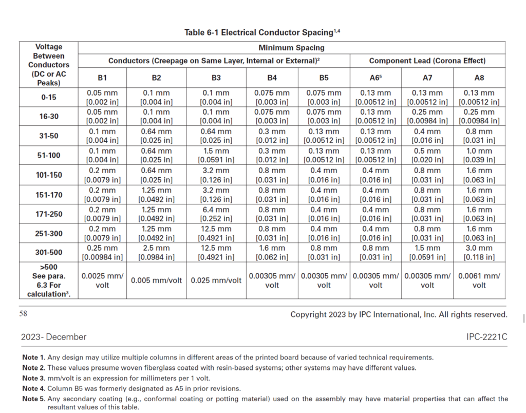
When it comes to designing PCBs, especially regarding recommended spacing guidelines for high voltage, the IPC standards are a great starting point and widely known as industry best practices. The foundation specification for PCB design is the IPC-2220 series. It establishes generic requirements for printed circuit board design. The most referenced standard for PCB spacing in high-voltage applications is IPC-2221, which outlines minimum spacing requirements based on working voltage. The latest revision of IPC-2221 is Revision C, released on December 14, 2023.
Key points from IPC-2221:
- Spacing requirements are provided for both internal layers and external layers.
- Table 6-1 in IPC-2221C (Figure 1 below) lists minimum electrical clearance distances in mils or mm, depending on the voltage and whether the spacing is internal or external.
- Additional adjustments are recommended when environmental factors such as pollution, humidity, or altitude are involved.
- For voltages greater than 500V, the (per volt) table values in Table 6-1 shall be added to the 500V values, utilizing the per volts modifier in each column. For example, the electrical spacing for Type B1 printed board with 600V is calculated as:
600V – 500V = 100V
0.25 mm [0.00984 in] + (100V x 0.0025 mm)
= 0.50 mm [0.0197 in] clearance
Additional optional but useful standards and references
While this blog focuses on practical design, some engineers may want to dive into the details of the standards:
- IPC-4101: Specification for Base Materials for Rigid and Multilayer Printed Boards
- IPC-4562: Metal Foils for Printed Board Applications
- IPC-6012: Qualification and Performance Specification for Rigid Printed Boards
- IPC-2152: Standard for Determining Current carrying Capacity in Printed Boards Design
- IPC-9592: Requirements for Power Conversion Devices for Computer and Telecommunications industries (While not focused specifically on PCB layout, IPC-9592 reinforces the importance of adequate spacing in power conversion devices, especially those operating at high voltage.)
- IEC 60664-1: International Standard (Covers insulation coordination, creepage, and clearance based on pollution degrees and material groups.)
- UL 796: Standard For Safety Printed-Wiring Boards (Governs safety of PCBs for UL certification.)
Key design factors that influence spacing
Practical guidance you can apply immediately in your design tool:
- Define high-voltage net classes with custom clearance rules.
- Use cutouts/slots in the PCB to increase creepage without taking more board space.
- Avoid right angles in high-voltage traces, prefer rounded corners.
- Separate High Voltage (HV) and Low Voltage (LV) circuits both physically and electrically.
- Use top (primary side) or bottom (secondary side) layers for high-voltage nets when possible, as its easier to enforce spacing and apply coatings.
- Label high-voltage areas clearly for assembly, testing, and inspection.
Do’s and don’ts
Do:
- Use your EDA tool’s features/capabilities such as the DRC engine to enforce spacing rules.
- Create a dedicated “HV” net class with increased clearance.
- Validate spacing visually and during layout reviews, to include consulting with your fabricator.
Don’t:
- Route high-voltage traces under components without adequate spacing.
- Assume default trace spacing is enough. Check and double-check!
- Ignore long-term effects of contamination or environmental exposure.
Final thoughts
PCB high voltage spacing isn’t just a checkbox, it’s one of the most critical safety measures you’ll build into your board. It goes beyond functional routing. It’s a safety-critical discipline that demands adherence to industry standards like IPC-2221. Whether you’re designing for a 100V power supply or a 1kV industrial controller, spacing matters. Understanding the difference between clearance and creepage, considering the operating environment, and applying industry best practices ensures your board is robust, reliable, and safe.
PCB high voltage spacing is one of those things that only becomes critical after it fails, but when it fails, it can be catastrophic. The good news? It’s avoidable! By understanding the difference between clearance and creepage, respecting the voltage-to-spacing relationship, and applying careful layout techniques and best practices, you can create high-voltage PCBs that are safe, stable, and built to last. By thinking carefully and doing your due diligence with regards to creepage, clearance, and layout strategy, you’ll protect your components, your users, and your reputation.