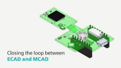
Closing the loop between ECAD and MCAD: seamless ECAD-MCAD collaboration through IDX and Xpedition
November 17, 2025
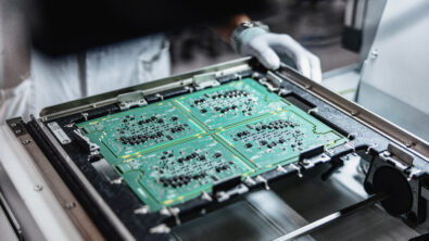
Unite electronic and mechanical design teams with Xpedition Standard’s built-in ECAD-MCAD collaboration. Discover how the IDX framework enables real-time synchronization, preserves design intent, and eliminates data bottlenecks for faster, error-free PCB development.