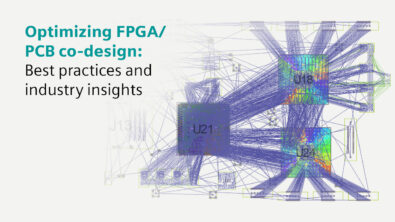
PCB design best practices: FPGA/PCB co-design
The next best practice in the model-based systems engineering pillar is FPGA/PCB co-design and optimization.
What is FPGA/PCB co-design?
FPGA/PCB co-design is an approach to designing electronic systems that combines the design of both the FPGA and the PCB into a cohesive and optimized process. This approach is especially important in today’s electronic product development process, where FPGAs are commonly used to implement customizable complex digital functions.
What’s not working?
FPGAs can be highly complex devices and come in an assortment of physical packages. This complexity can also lead to longer development times, increased engineering cost, and increased chances of design errors.
High-performance FPGAs can consume significant power, especially when running complex algorithms or processing large amounts of data. Managing power distribution and thermal considerations, along with addressing optimization of pin assignments, can be challenging when designing a PCB.
Best practices: FPGA/PCB co-design
Use a tool that enables correct-by-construction FPGA I/O assignment, allowing pin swapping and layout-based I/O optimization within the PCB design process.
FPGA/PCB co-design is critical for optimizing the performance, reliability, and manufacturability of electronic systems that incorporate FPGAs. This integration between the multiple disciplines and their respective domains ensures that both the hardware and the FPGA-based digital logic are designed in harmony to create a high quality functional and efficient electronic product.
You can also reduce or prevent EMI or SI issues with a tightly integrated flow, which removes the potential for errors, the need for respins, and reduces risks.
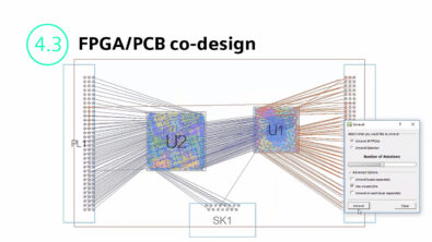
How it works: FPGA/PCB co-design
When using an FPGA in a design, bridging the gap between the FPGA and PCB domains is crucial for optimizing the FPGA IO within the context of the board. Using the FPGA, PCB co-design functionality of Xpedition, groups of signals can be created easily to manage the complexity of high pin count FPGAs and accelerate the pin assignment process. This manageability positively influences the trace routing stage where an optimized pin assignment ensures ease of pin escapes and trace routing of the FPGA. In the end, this leads to increased overall performance of the PCB design.
These groups can be treated as separate HDL entities within the tool and can be created manually or extracted from an HDL file during the component placement and orientation on the board Floor. Planning using the FPGA PCB co-design can be done before and during the PCB layout process. Users can also make FPGA pin assignment changes to optimize routing.
Early on, this can result in fewer net line crossovers. However, during the entire design process the benefits can include reducing layers, minimizing signal integrity issues, shortening traces, and reducing the number of vias used.
Learn more on our FPGA/PCB co-design webpage or watch this short video: