PCB design best practices: Designing for advanced manufacturing technologies like rigid-flex PCB design and High-Density Interconnect
The next best practice I want to discuss as a part of engineering productivity and efficiency is designing for advanced design technologies such as rigid-flex PCB and high-density Interconnect (HDI).
What is rigid flex PCB design?
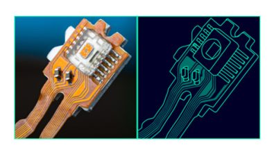
A rigid-flex PCB design typically consists of flexible substrate material along with rigid substrate material all constructed together to create one single design. This could include one or more sections of flex material along with one or more sections of rigid material. Utilizing this combination of rigid and rigid-flex structures, allows for a higher potential for addressing increased design complexity and challenges that come along with designing large systems that consist of multiple printed circuit board assemblies (PCBAs), or designing for confined physical/mechanical constraints within the specified design envelope.
Some of the pros for implementing a rigid-flex PCB design is the potential for removing connectors, increased SI performance and reliability by eliminating signal impedance mismatching as signals traverse through connectors. Improved electromechanical functionality due to its ability of the flexible material to dynamically bend to accommodate its final form factor and be more durable in meeting final product design requirements such as Highly Accelerated Stress Testing (HAST) and or Highly Accelerated Life Testing (HALT).
Within a rigid-flex PCB design, you can have multiple PCB stack ups in the respective sections, all within the same board design. The rigid area could potentially contain one stack up, while in the flex area, another PCB stack-up could exist. This can cause a lot of confusion, especially if you’re not sure of the design details, and or if you’ve never done it before (lacking the experience with rigid-flex PCB designs). So, when you think about a rigid-flex design, it’s still one PCB design, but containing a rigid section, and a flex section, with multiple PCB stack-ups for the respected sections, all in one design to accommodate a specific form, fit, or function requirement and to meet electromechanical functionality of the final product. Rigid-flex and flex designs are typically utilized in products commonly see in aerospace, automotive, medical, and military applications.
What is High Density Interconnect (HDI)?
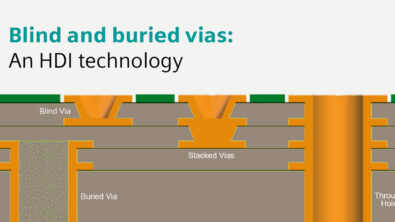
High Density Interconnect (HDI) is miniaturization of a printed circuit board (PCB) containing a high number of interconnects in a minimal amount of space. Typically, tighter component spacing, and pin-pitch leads to the utilization of HDI which includes smaller traces, smaller spaces, blind (vias that make a connection by starting from an external layer and ending on an internal layer only, or vice-versa) and buried vias (vias that make connections on internal layers only, where these vias structures never get exposed to the primary and secondary layers) that may require smaller drill sizes known as microvias with holes typically 0.006” or smaller.
It’s one of the fastest growing PCB technologies for many years now. Everything in the industry continues to get smaller and smaller such as component packages and their respective pin-pitches, signal trace routings, and increased overall board density.
What’s not working?
When it comes to rigid flex PCB design, many people just don’t know what the full capabilities are in their eCAD tool. They’re a bit hesitant or reluctant to go with these design structure options due to inexperience implementing, and or lack of comprehension/knowledge of this advanced manufacturing technology.
When we talk about HDI, the problem is, that many people are still using the standard via structure when they could be taking advantage of implementing HDI in their approach on their designs. With that said, you must know and understand that there are gives and takes (pros and cons). Also, many are not communicating with their PCB supplier early in the design process, especially when implementing HDI in the design. This lack of understanding and or experience along with lacking upfront communication leads to potential downstream issues.
What are the roadblocks?
Typical roadblocks that prevent many from implementing advanced design technologies is unfamiliarity and or inexperience with rigid flex PCB or flex PCB design. The same roadblocks exist with how to incorporate HDI. Most of time, all it takes is a simple phone call to their fabricator to get a better understanding, get direction, and validate if these technologies are an option to better suit their needs.
Another problem that I see is that people think that implementing advanced technologies requires hiring a subject matter expert. It doesn’t! You just need to collaborate up front (early on), and throughout the design process with your PCB supplier. With regards to HDI specifically, there’s inefficient internal processes and or legacy methodologies that reduce the opportunity to implement HDI.
Best practices: rigid-flex PCB design and high-density interconnect (HDI)
Best practices for rigid-flex PCB design, really takes advantage of the rigid flex capabilities and advanced features within your respective tool sets to enable efficient ways to define board outline, the multiple PCB stack ups for the respected sections of the design, and regional constraints. Most of today’s EDA tools are more than capable of implementing these advanced design techniques that include both the rigid section(s) and flex section(s) all in one board outline, where they are all collectively treated as one single design.
Legacy methodologies may utilize multiple databases to accomplish the same results, or worse, these advanced features are not available in your respective EDA tools. When we think about what kind of value this brings to your design process, you now have a higher potential for achieving success with designing complex PCBs, and a more efficient way to design complex systems. As an example, implementing rigid-flex has the potential of optimization of signal flow from board-to-board connection by way of eliminating those costly board to board connectors that those signals are required to go through as signals traverse back and forth, from one board to another. Plus, there is the added ability to implement and meet complex requirements within your design.
In high pin count components such as BGAs, especially as the pin pitch gets tighter and tighter with these smaller component packages, there is no choice. You must implement HDI to get all required pin escapes in place for signal routing. The decision to implement HDI in your design may be made without even realizing it. For example, a certain component may have been selected during the schematic creation process, and that component happens to have a very small pin pitch that automatically requires the implementation of HDI to design in this part.
On the positive side, HDI eliminates legacy design workarounds as well as having the ability to add increased complexity to your designs, such as implementing high pin count connectors, devices containing higher IO capability, and smaller component packages.
How it works: rigid flex PCB design
Having native support for technologies like rigid-flex can be essential for designs where board real estate is limited, and component density extremely high.
To expedite a rigid flex design, the entire board outline that includes both rigid and flex sections of the design can be imported directly from MCAD, and a qualified manufacturing stackup can be imported directly from HyperLynx. Within the PCB stackup, these defined layers can then be assigned to the different sections within the board outline in the design, which are used to manage the separate rigid and flex regions of the board.
For more advanced designs, once the designer has moved on to placement, buried cells can be placed on internal flex layers of the board.
How it works: high density interconnect (HDI)
When it comes implementing HDI, meeting with your PCB supplier upfront and qualifying an agreed upon PCB stack that may include such details as a layer count, specific material and copper weight, board thickness, impedance requirements, standard through hole vias, blind vias, buried vias, and micro-vias to meet your design intent/requirements.
By utilizing HDI, you increase your ability to have a much greater density in a smaller footprint. It enables you to rout signal traces through very small component pin-pitch fields and through high component density areas of your board. The key here is to optimize the signal flow as the signal’s traces traverse through the multiple layers of the PCB. HDI increases the ability of making connections from one layer to another by utilizing blind or buried vias, or microvias where via fan-out is simply impossible or via-in-pad is required. The main take away for using HDI is that we gain the ability to strategically connect only certain pads on certain layers, which greatly reduces the need for board real estate.
To learn more about designing for advanced manufacturing technologies like rigid-flex PCB design and High-Density Interconnect visit our website or watch this video.