Bridging the gap: Unlock seamless collaboration in IC design with Calibre Connectivity Interface
By Samar Abd El-Hady & Wael ElManhawy
The world of integrated circuit (IC) design is a whirlwind of innovation, constantly pushing boundaries with shrinking geometries and mind-boggling complexity. In this fast-paced environment, no single tool can do it all. The secret to success? Seamless collaboration between Electronic Design Automation (EDA) tools. It’s no longer a nice-to-have; it’s an absolute necessity.
Enter Calibre Connectivity Interface (CCI) – your critical integration hub.
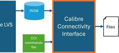
Think of Calibre Connectivity Interface (CCI) as the ultimate translator and data highway for your EDA ecosystem. It acts as a central bridge, facilitating efficient workflows by connecting verification, analysis and design tools through a common protocol (figure 1).

At its core, CCI is a powerful interface that leverages the output of a Calibre LVS (Layout vs. Schematic) run. When Calibre LVS verifies your design, it generates a comprehensive database called the Standard Verification Database (SVDB). Calibre’s CCI taps into this SVDB to extract crucial information such as:
- Layout shapes
- Nets and devices
- Rule file configurations
- Corresponding schematic or source names
This rich, verified data then becomes accessible to other downstream tools, ensuring consistency and accuracy across your entire design flow. The well-established CCI flow gives these silicon modeling and analysis tools direct access to the extracted layout connectivity information, making your design process smoother and more reliable.
CCI’s superpower: Seamless integration with diverse applications
The true strength of CCI lies in its profound ability to seamlessly integrate with a wide and diverse ecosystem of third-party tools and existing design workflows. This means information flows freely, reducing errors and rework, enhancing accuracy and ultimately streamlining your workflows for faster time-to-market.
Key applications and integrations of Calibre CCI
Enhancing parasitic extraction flows
Parasitic extraction tools are often primary integration points for CCI. These tools demand access to critical design data, including geometric layouts, connectivity details, net and instance names and device and port information. CCI is specifically engineered to provide all this essential data, enabling the accurate generation of parasitic models crucial for completing your physical verification flow.
CCI offers a robust and flexible set of APIs, allowing various third-party parasitic extraction tools to precisely query and retrieve the specific data they need. This includes successful interfaces with:
- Empyrean’s PEX tool: Reads CCI data to generate layout analysis with parasitic RC and critical path netlists.
- Phlexing’s GloryEX extraction tool: Generates parasitic netlists and structure files, supporting 3D modeling for advanced devices like FinFET and GAA, and crucial for sign-off flows.
- Synopsys StarRC and Cadence QRC tools: Benefit from dedicated CCI APIs that allow real-time access to device-level layout data, robust SPICE model correlation, geometry-to-schematic mapping and integration into full-chip sign-off flows.
Accelerating high-frequency verification
For high-speed designs, evaluating electromagnetic (EM) behavior of critical signal paths is vital. Siemens EDA partnered with Lorentz Solution, Inc. to integrate Calibre nmLVS with Lorentz PeakView products using CCI. This powerful combination creates a high-frequency design flow that delivers ease of use and enables IC and 3D IC designers to develop post-layout solutions correlated with source/schematic names, devices and hierarchy.
Improving power integrity analysis
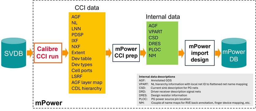
CCI has achieved a robust and successful integration with mPower, Siemens’ comprehensive power integrity solution. mPower provides scalable analysis for digital, analog and complex 3D IC architectures. CCI is a key enabler for this synergy, seamlessly providing all essential input data to the mPower flow, including Annotated Geometry Files (AGF), detailed device data and cross-reference files. This ensures accurate and efficient execution of high-resolution voltage drop (IR) and EM analysis, full-chip power grid modeling and accurate power pin annotation.
Streamlining transistor radiation simulation
For critical reliability analysis, CCI has successfully interfaced with IROC Technologies, a leader in soft error analysis. Their TFIT (Transistor Failure in Time) tool requires precise transistor drain and source diffusion coordinates from GDS files to perform cell-level soft error analysis. By integrating with Calibre nmLVS via Calibre CCI, a new, reliable and automated flow is created to:
- Extract accurate drain/source locations.
- Execute the TFIT flow with precise input data.
- Eliminate previous technical limitations.
- Streamline the entire analysis process.
This transformation ensures that vulnerable zones within the design are accurately identified, enhancing overall system reliability.
Real-world applications: Calibre CCI in action
To understand the practical value of Calibre CCI, consider these use cases:
- Automotive IC sign-off: By combining parasitic extraction (e.g., with StarRC) and soft error rate (SER) analysis (with TFIT), CCI ensures functional correctness and reliability over extended temperature and voltage ranges, critical for automotive applications.
- 3D IC integration: For 2.5D/3D IC stacks, CCI simultaneously feeds tools like mPower for package power analysis and GloryEX for interposer parasitic extraction, providing a comprehensive view of complex multi-die systems.
- Analog-mixed signal design: Designers leverage CCI for essential tasks like EM validation, parasitic-aware simulation and accurate noise coupling prediction with various third-party tools, crucial for sensitive analog circuits.
Conclusion: Your universal bridge to multi-tool integration
In today’s complex integrated circuit design landscape, seamless collaboration between EDA tools is no longer optional but essential. The Calibre Connectivity Interface serves as a critical integration hub, enabling efficient data exchange and communication across diverse design and verification workflows.
By leveraging the comprehensive data from Calibre LVS, CCI provides a robust foundation for advanced analyses. As demonstrated through its successful integrations with leading third-party tools, CCI consistently proves its versatility and critical role.
Ultimately, Calibre CCI transforms LVS into a powerful data source for a wide array of specialized tools. This foundational integration technology significantly enhances design accuracy, streamlines complex verification cycles and accelerates time-to-market for cutting-edge IC and 3D IC designs, proving indispensable for future semiconductor innovation.
Ready to unlock the full potential of your EDA ecosystem? Explore how Calibre CCI can transform your design flow and empower key design workflows through downloading our technical paper CCI: Your universal bridge to multi-tool integration | Siemens Software
Frequently Asked Questions about Calibre Connectivity Interface (CCI)
Q1: What is the Calibre Connectivity Interface (CCI) and why is it important for IC design?
A1: The Calibre Connectivity Interface (CCI) acts as a critical integration hub and a “data highway” for your Electronic Design Automation (EDA) ecosystem. In today’s complex IC design world, no single tool can do everything, so seamless collaboration between different tools is essential. CCI bridges this gap by facilitating efficient workflows and communication between verification, analysis, and design tools through a common protocol. It’s important because it enables consistent data exchange, reduces errors, and ultimately streamlines design workflows for faster time-to-market.
Q2: How does CCI work, and what kind of data does it provide to other tools?
A2: At its core, CCI leverages the output of a Calibre LVS (Layout vs. Schematic) run. When Calibre LVS verifies a design, it generates a comprehensive database called the Standard Verification Database (SVDB). Calibre’s CCI taps into this SVDB to extract rich, verified data. This includes crucial information such as layout shapes, nets and devices, rule file configurations, and corresponding schematic or source names. This extracted data then becomes accessible to other downstream tools, ensuring consistency and accuracy across the entire design flow.
Q3: What are some key applications and benefits of using Calibre CCI in IC design?
A3: The true strength of CCI lies in its ability to seamlessly integrate with a wide range of third-party tools and existing design workflows. Key applications and benefits include:
- Enhancing Parasitic Extraction Flows: CCI provides essential data (geometric layouts, connectivity, names, device info) to parasitic extraction tools, enabling accurate generation of parasitic models for physical verification.
- Accelerating High-Frequency Verification: It enables powerful high-frequency design flows by integrating with tools like Lorentz PeakView, allowing for post-layout solutions correlated with source/schematic names.
- Improving Power Integrity Analysis: CCI seamlessly provides all necessary input data to solutions like Siemens’ mPower for accurate and efficient high-resolution voltage drop (IR) and EM analysis.
- Streamlining Transistor Radiation Simulation: It creates automated flows for tools like IROC Technologies’ TFIT, providing precise transistor drain/source coordinates for cell-level soft error analysis, enhancing reliability.
Ultimately, CCI transforms LVS into a powerful data source, significantly enhancing design accuracy, streamlining complex verification cycles, and accelerating time-to-market for cutting-edge IC and 3D IC designs.
