Revolutionizing 3D IC design with integrated multiphysics verification
By Yoyo Li
The semiconductor landscape is always evolving—sometimes quietly, sometimes at breakneck pace. Today, as integrated circuit designs progress from established 2D layouts to sophisticated 3D architectures, new challenges and opportunities are emerging for silicon engineers. These new architectures are not just denser and more powerful; they also unlock entirely new forms of inter-layer electrical, thermal and mechanical interaction. Success in this new world depends on more than incremental improvements—it requires an integrated, system-level, multiphysics verification approach.
Beyond the boundaries of 2D: Why 3D ICs need a new verification mindset
Historically, the industry thrived on 2D process scaling and established verification flows. 2D methodologies defined the rules for decades, giving engineers predictable tools and workflows. However, escalating performance, power and bandwidth demands—and the onset of system-in-package and heterogeneous integration—are now pushing chipmakers toward breakthroughs in 3D integration.
The shift to 3D is about more than stacking dies. It involves:
- Routing high-speed signals vertically and horizontally across different substrates
- Managing heat threats from localized power densities
- Balancing stress profiles to protect delicate structures
- Validating heterogeneous assemblies—often built with dies on differing process nodes
Each of these aspects introduces complex failure modes. These cannot be captured by legacy approaches. Addressing these challenges requires solutions that fully embrace the realities of multiphysics design and verification.
Learn more in our latest technical paper, A comprehensive approach to 3D IC physical verification: DRC, LVS and beyond.
Siemens EDA: Redefining multiphysics verification
Siemens Digital Industries Software (Siemens EDA) recognized these evolving needs and invested in building a cohesive, extensible 3D IC verification ecosystem. This includes:
- Calibre 3DStack: For full 3D DRC, LVS and connectivity
- Calibre 3DThermal: Advanced thermal simulation
- Calibre 3DStress: Package and transistor-level mechanical analysis
- mPower power integrity: EM/IR integrity analysis
Together, these tools extend beyond the capabilities of siloed domain solvers, enabling deep, accurate and early assessment of 3D multiphysics risks—saving time and reducing late-stage surprises.
The Calibre 3D IC solutions are part of the larger Siemens EDA 3D IC portfolio (figure 1).
Mastering complexity: A deeper look at Calibre 3DStack
In 3D IC design, design rule checking (DRC) and layout versus schematic (LVS) are critical verification steps that ensure the manufacturability and electrical correctness of the design. With the growing influence of multiphysics effects, these checks must be performed alongside additional analyses of thermal and stress domains, providing a holistic view of project risks and performance. Calibre 3DStack empowers designers by:
- Handling giga scale GDS and netlist datasets with hierarchical processing
- Enabling consistent DRC/LVS checking across multiple process nodes and technologies
- Integrating with Siemens Innovator 3D IC Integrator for seamless design data hand-off
- Implementing fan-out design layout by Xpedition and SoC design layout by Aprisa
- Generating precise, actionable error reports that speed up closure
DRC/LVS and interconnectivity requirements are enforced not just at the die level, but also at every interface—across chiplets, interposers and package surfaces. This holistic approach significantly reduces risk.
Precision thermal modeling with Calibre 3DThermal
Thermal issues can erode performance and reliability in stacked dies. Traditional lumped models often miss subtle interactions. Calibre 3DThermal introduces:
- Hierarchy-aware, instance-level power mapping from RTL through implementation
- Accurate materials mapping to capture the effects of die thinning, underfill and advanced packaging
- Solver acceleration via integration with Simcenter Flotherm
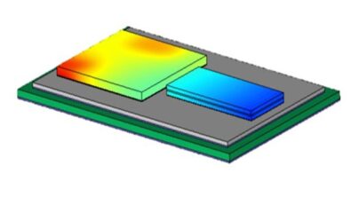
Calibre 3DThermal enables teams to iteratively explore thermal gradients and adjust floorplans, block placements, or cooling solutions—lowering design risk and optimizing for both yield and long-term system health. Figure 2 shows the thermal results after simulation in Calibre 3DThermal, along with a composite materials map and a power map.
Mechanical reliability with Calibre 3DStress
Modern packages involving through-silicon vias (TSVs), copper pillars and non-planar dies face unique mechanical risks. Calibre 3DStress empowers designers and packaging experts to:
- Simulate die warpage, thermal expansion and piezoresistive effects during early floor planning
- Visualize risk at both the block and device level—down to the transistor
- Enable what-if analysis to optimize die stacking orders, materials and bump layouts
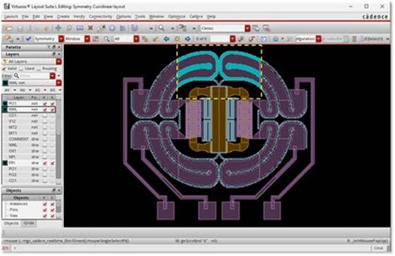
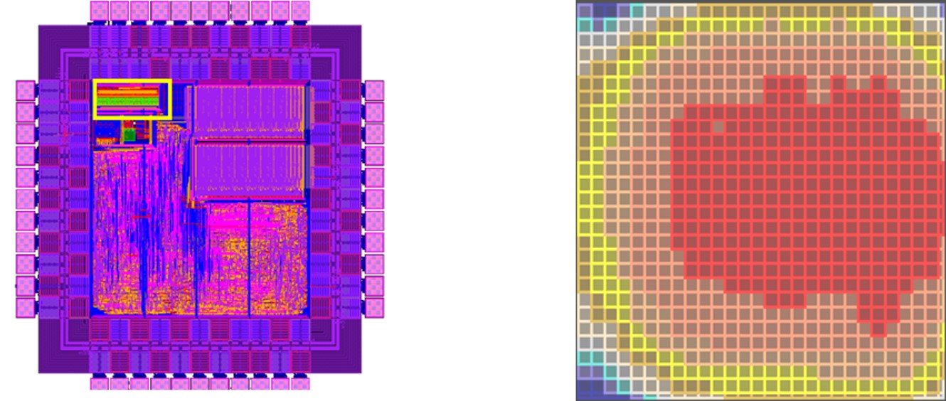
Conducting stress analysis early can mitigate package-induced failures, reduce overdesign and prevent loss of yield. Full-chip and block-level visualizations reveal potential hotspot locations, allowing design teams to proactively address mechanical reliability concerns and make informed trade-offs (figure 3).
Learn more about Navigating 3D IC stress: physical realities and best practices for 3D IC reliability.
Addressing EM and IR drop in dense 3D systems
Electromigration and IR drop are rapidly escalating concerns as more current flows through thinner interconnects. The Calibre mPower solution provides:
- Automated current density extraction across 3D pathways, interposers, TSVs and redistribution layers
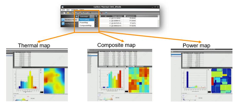
- Visualization tools to immediately relate EM/IR risk back to physical design, as shown in figure 4
- Data-driven optimization to help teams balance performance and reliability across operating conditions
Learn more about mPower in this brief overview video.
From isolated analysis to integrated, team-based workflows
One of Siemens’ biggest advantages is cross-flow integration. Modern 3D IC projects are team sports, requiring constant communication among silicon architects, package designers and reliability engineers—sometimes spread across regions and organizations.
With Calibre’s interoperable environment:
- Design and verification data can be shared and probed interactively across all domains
- Schedule risks and design closure bottlenecks are minimized
- Automated report generation, process-specific rule decks and result databases provide transparency and audit trails for management
Building the future of 3D IC: Reliability, speed, confidence
From system ideation through bring-up, 3D IC verification with Siemens EDA enables:
- Proactive detection of multiphysics issues
- Accelerated design closure with fewer spins
- Higher confidence across design and manufacturing teams
By embedding multiphysics analysis into every stage of the flow, you save time, improve reliability and empower teams to focus on innovation.