Siemens acquires Canopus AI: Supercharging semiconductor manufacturing with AI-powered metrology
The semiconductor industry is a relentless race for smaller, faster and more efficient chips. As device geometries shrink to atomic scales, the challenges in manufacturing become exponentially complex. That’s why we’re thrilled to announce a significant strategic move that will empower semiconductor manufacturers to overcome these hurdles: Siemens has acquired Canopus AI, a leading innovator in computational and AI-powered metrology and inspection solutions.
This acquisition isn’t just about growth; it’s about accelerating the future of semiconductor manufacturing.
Why Canopus AI is a game-changer for Siemens and the industry
The combination of Siemens’ robust Calibre™ Computational Lithography and Manufacturing Physics Simulation platform with Canopus AI’s cutting-edge metrology and inspection technologies creates a truly differentiated, end-to-end electronic design automation (EDA) solution.

“The acquisition of Canopus AI exemplifies Siemens’ commitment to leveraging industrial AI to solve critical challenges in semiconductor manufacturing,” says Tony Hemmelgarn, CEO Siemens Digital Industries Software.
What does this mean for our customers?
- Improved fidelity of printed wafer patterns: Get closer to perfect designs on every wafer.
- Accelerated yield ramp: Bring new products to market faster and more efficiently.
- Reduced time-to-volume for advanced nodes: Stay ahead in the competitive landscape.
This integration is a leap forward in our vision of a high-accuracy semiconductor manufacturing digital twin, enabling unparalleled sub-nanometer process control and mask development.
The strategic importance: AI meets the angstrom era
The semiconductor industry faces immense pressure. As we push into the angstrom era, where dimensions are measured in fractions of a nanometer, “massive metrology” – the precise measurement and analysis of structures – becomes absolutely critical for ensuring quality and yield.
Canopus AI’s innovative AI-powered solutions perfectly complement Siemens’ existing portfolio. They provide manufacturers with intelligent inspection and measurement capabilities that are essential for driving operational excellence in this demanding environment.
This acquisition underscores Siemens’ commitment to leveraging artificial intelligence to solve the most critical challenges in semiconductor manufacturing. By merging Canopus AI’s specialized expertise with Siemens’ industry-leading infrastructure and extensive customer relationships, we are uniquely positioned to deliver the next generation of metrology and inspection software solutions that manufacturers will come to depend on.
Read about AI in Calibre Manufacturing
Diving deeper: The power of Canopus AI’s technology
Founded in 2021, Canopus AI has quickly established itself as a revolutionary force in wafer and mask metrology and inspection. Their vision is to move towards “metrospection” – a seamless marriage of conventional metrology and inspection – using a comprehensive AI-driven software framework to meet the extreme precision requirements of advanced technology nodes.
Cutting-edge deep learning-based metrology & inspection software platform
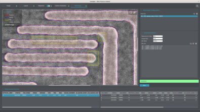
Canopus AI specializes in massive ebeam metrology, offering unprecedented data throughput and accuracy for OPC/RET (optical proximity correction/resolution enhancement technology) applications. Their solutions are instrumental in achieving optimal lithography performance, pushing the boundaries towards the angstrom era. This powerful platform enables:
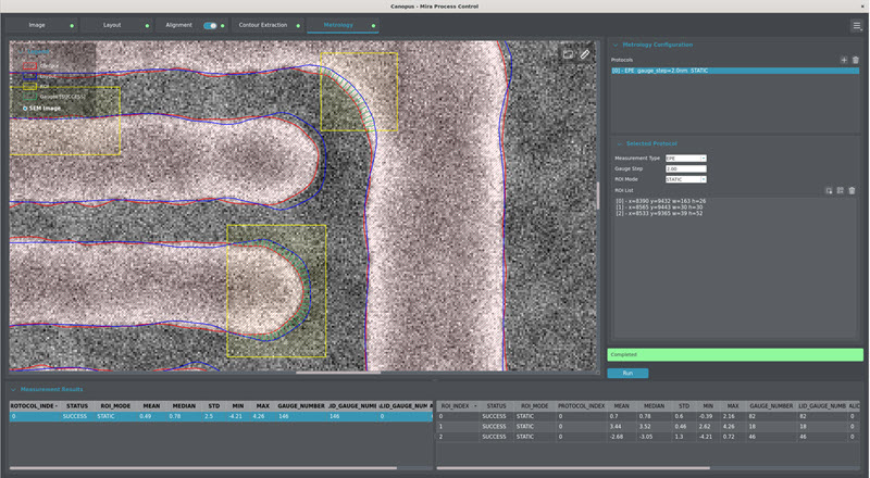
- Robust EPE (edge placement error) based measurements.
- Early identification of critical defects.
- Extensive characterization of process variations and stochastics.
From 2D to 3D insight
Canopus AI extends its expertise beyond 2D, offering advanced TEM (transmission electron microscopy) metrology for crucial 3D insights. This capability is powered by a unique engine for synthetic 2D and 3D SEM (scanning electron microscopy) image generation, leveraging state-of-the-art AI and machine learning algorithms. This allows for:
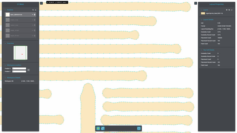
- Computational metrology and inspection platform: Handling data from vertex-based to pixel-based geometries.
- Multigon data support and native curvilinear data operations: Best-in-class CD SEM image processing algorithms, including ML and AI, for metrology and inspection.
- Massive metrology processing workflow: Easy recipe tuning and automatic processing of hundreds of thousands of CD SEM images, from data filtering to gauge-based or EPE-based measurements.
- SEM EPE metrology for OPC/RET: Integrating Canopus AI’s SEM contour extraction technology with Calibre’s industry-leading contour-based OPC/Etch ML model calibration, achieving angstrom-level model accuracy with superior runtime.
- Process window characterization: Automatic process window calculation from SEM images collected under different focus and dose conditions.
- Curvilinear masks metrology using CDSEM images.
- Manufacturing process control: Monitoring minute changes in SEM image contour during chip manufacturing.
- From 2D SEM metrology to 3D TEM metrology: Addressing the need for 3D profile information in many memory applications for process development or process control.
- Synthetic SEM and TEM generation engine: An AI-based engine capable of handling large SEM acquisition conditions and creating synthetic SEM images for AI training, programmed defects generation and D2DB data flow.
A bright future for semiconductor innovation
We are incredibly excited to welcome the talented Canopus AI team to Siemens. Their expertise will be instrumental in driving the next wave of innovation in metrology for semiconductor manufacturing, helping our customers achieve unprecedented levels of precision, efficiency and yield in the angstrom era.
Suggested Links:
- More about computational lithography: Enhancing EUV lithography resolution at high numerical aperture (blog)
- Glossary of semiconductor terms (OPC, EPE, etc.): https://www.lamresearch.com/technical-glossary/


